1432
A high current, in-bore, switched capacitor voltage converter with low EMI and high efficiency.1Skope Magnetic Resonance Technologies AG, Zuerich, Switzerland
Synopsis
Keywords: New Devices, New Devices, In-bore electronics
Motivation: Due the noise emission of switch mode power supplies, linear regulators are often present in electronics in and around the MR bore, with the related thermal challenges.
Goal(s): In this work we present a switched capacitor converter witch is capable of providing high output currents without emitting noise in the MR RF band.
Approach: The goal was achieved by controlling the slew rate of the gate source voltage of the switching GaN FETs.
Results: High efficiency, low output ripple and no unexpected transient behavior could be measured on the bench.
Impact: The presented 10A switched capacitor converter can provide efficiently power to electronics without emitting RF noise around the MR RF band. Enlarging the integration possibilities of high density electronics in and around the MR bore.
Introduction
Increasingly more system components of an MR installation and accessories are placed either in the MR bore or around magnet. Modern low power electronics trends towards lower and multiple., specific voltage rails with comparably high current requirements. In most applications this challenge is addressed by inductive switch-mode power supplies (SMPS) such as a buck converter. However, such buck converter typically emit a significant amounts of noise in the RF band of a MRI system[1] particularly if a high efficiency is required. Hence, designers often revert to linear and low-dropout (LDO) for in-bore applications inflicting increased power losses and heat deposition. An alternative, to SMPS are switched capacitor converters (SCC). These converters have been shown to emit very little to no noise in the RF band[3], however, they were limited to only small currents. In this work, we show that a SCC design both emits very low RF noise and is capable of up to 10A output currents enabling the efficient supply of high current electronics inside or in the vicinity of the MR bore. The implementation of the SCC features a divide-by-two converter followed by a cascaded divide by-two-converter and a cascaded divide-by-two-thirds converter. Therefore the input to output conversion rations are 1/2, 1/3 and 1/4.Methods
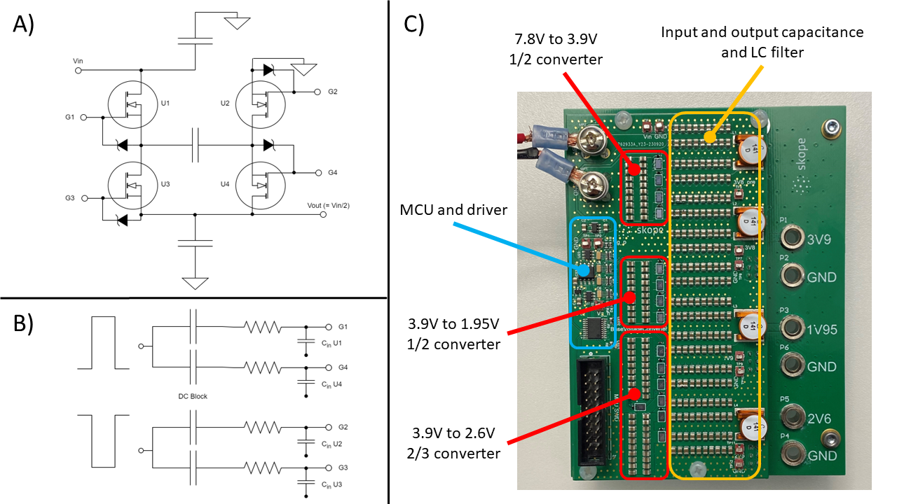
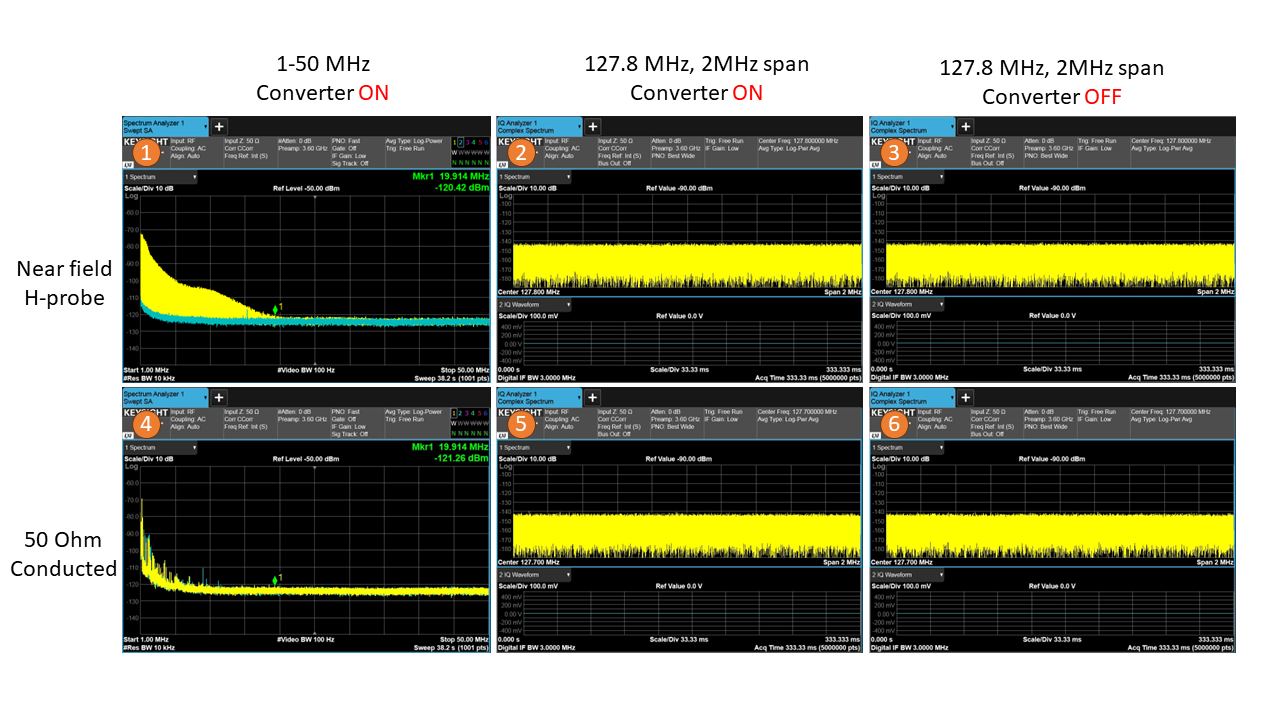
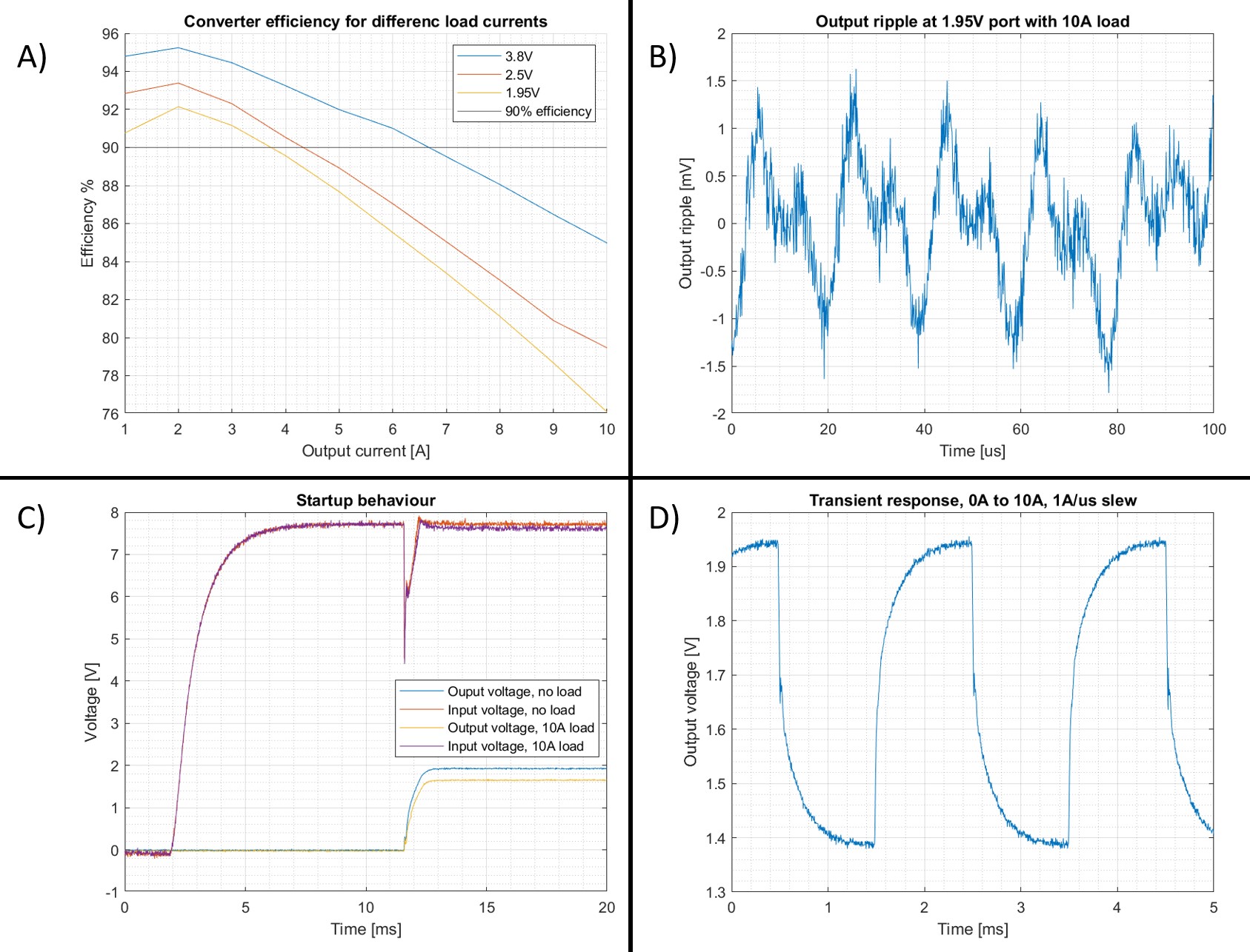
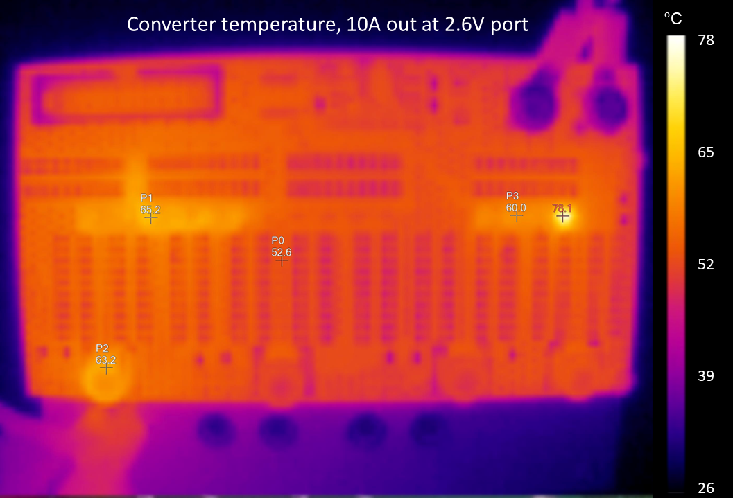
The topology of the divide-by-two converters is shown in Fig. 1A with EPC2055 GaN FET as switching elements. To suppress the RF noise which is the most problematic when a switch opens or closes, the gate drive circuitry was adapted to have a large resistance in series (Fig. 1B) limiting the rise and fall rate of the gate source voltage. Therefore, the switches are opened and closed slowly to suppress the high frequency components to a great amount. The implementation of the converter board on top of a breakout board is shown in Fig. 1C. Tuning of the component values to achieve a good balance between efficiency and noise performance was done with a spice simulation in LTSpice. The RF noise performance of the converter, shown in Fig. 3, was measured with a Keysight EXA N901B signal analyser, a R&S HMP4030 power supply and a Siglent SDL 1020X-E electronic load. The converter was placed into a shielded RF chamber and RF noise was measured either with a H-Field probe or on the output leads to get the conducted emission. The performance characteristics of the converter were measured on the bench with a R&S HMP4030, Siglent SDL 1020X-E, Siglent SDM3065-SC and Keysight DSOX4054A. Plotted in Fig. 4 are the converter efficiency, output ripple at 10A load, startup behavior and transient load response. The thermal performance was evaluated with a Fluke PTi120 thermal imager while pulling 10A from one of the converter outputs.Results
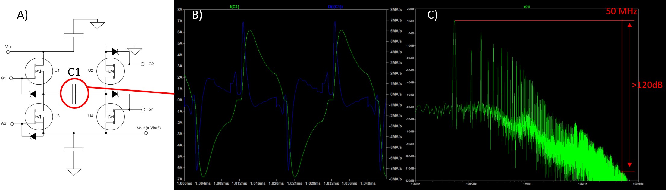
The spice simulation, showed that the peak current through the capacitor is around double the output current and that for even 3.2A load the maximum derivative of the current is less than 10A/us as shown in Fig. 2B. Fig. 2C shows the spectrum of the current through C1 and as can be seen there, relative to the main peak the switching frequency at 50kHz, any frequency components above 50MHz are at least be a factor of 120dB smaller than the main peak. As can be seen in Fig. 3 no RF noise neither conducted nor in the magnetic near field on top of the converter can be measured above 20MHz. Furthermore, in the MR RF band of 127.8 MHz with a span of 2MHz no change in the noise floor between converter on and off could be observed. In the bench measurement, shown in Fig. 4, it could be shown that an efficiency of at least 90% could be achieved for high currents up to 6.5A for the first converter. Very little output ripple of 1-2mV could be measured even with 10A output load. During startup and sudden load transients no overshoot or otherwise unexpected behavior could be observed. The design can handle 10A output current thermally as shown in Fig. 5. The hotspot in the design is GaN FET U1 in the first converter.Discussion and conclusion
A MR compatible switched capacitor converter could be shown that can handle high output current and low/no RF noise on the MR bands. Controlling the slew rate of the GaN FET gates was shown to be sufficient to suppress the RF noise to an adequate amount.Acknowledgements
No acknowledgement found.References
[1] Vogt, C. (2017). Design Concepts and Validation of In-field MRI Electronics (Doctoral dissertation, ETH Zürich, Zürich, Switzerland). Retrieved from https://doi.org/10.3929/ethz-b-000246692
[2] J. Reber et al., "An In-Bore Receiver for Magnetic Resonance Imaging," in IEEE Transactions on Medical Imaging, vol. 39, no. 4, pp. 997-1007, April 2020, doi: 10.1109/TMI.2019.2939090.
[3] Schildknecht C.M. et al, In-bore voltage inversion with very low EMI by a switched capacitor converter, Proc. Intl. Soc. Mag. Reson. Med. 28 (2020), 1133
Figures