4553
An in-bore PIN diode driver based on a single chip with nanoseconds rise/fall time1Institute for Biomedical Engineering, ETH Zurich and University of Zurich, Zürich, Switzerland, 2Center for Magnetic Resonance Research, University of Minnesota, Minneapolis, MN, United States
Synopsis
Keywords: New Devices, New Devices
An in-bore PIN diode driver with eight output channels is presented here. The driver is based on a single-chip solution making the implementation simple and of high performance. The rise and fall times of the driver's output are in the single-digit nanosecond range with a peak output current of up to 5.7A per channel. Triggering the driver can be done either with an optical or electrical signal. The driver was tested on the bench and in-bore of a 10.5T MR scanner.Introduction
PIN diodes have proven to be one of the workhorses in switchable MR radio frequency (RF) hardware[1]. They have found widespread use in transmit/receive (TR) switches[2-5], coil detuning circuits[1], and switchable attenuators[3]. There are multiple ways to configure a PIN diode in a circuit; however, the low voltage mode1 is often used as no hazardous high voltages are required when the MR system transmits RF power. In the low voltage mode, one often encounters a tradeoff between RF power handling capability and switching speed. However, in fast T2 sequences such as ZTE[6-10] or SWIFT[11-13] both high peak RF power and fast switching speeds are required. This tradeoff can be alleviated to a certain degree with a PIN diode driver that switches the bias voltage rapidly, provides high peak current capability, and a large reverse voltage. Unfortunately, a PIN diode driver with such characteristics is not always available as either the system-integrated driver is not up to the required specifications or a custom RF chain is used. To overcome this issue, dedicated PIN diode drivers[14] or RF hardware components with integrated drivers[2,15] have been developed. However, those PIN diode drivers are either customized to a specific use case, complex in their implementation, or not as fast as desired.In this work, we present a rapid in-bore PIN diode driver, where the all bias voltage switching is implemented in a single chip. This could be achieved by identifying that MOSFET gate drivers share many design requirements, such as fast switching speeds, high peak current, and high voltage swing.
Methods
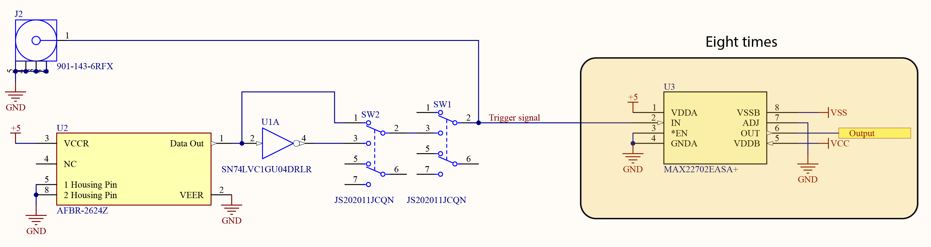
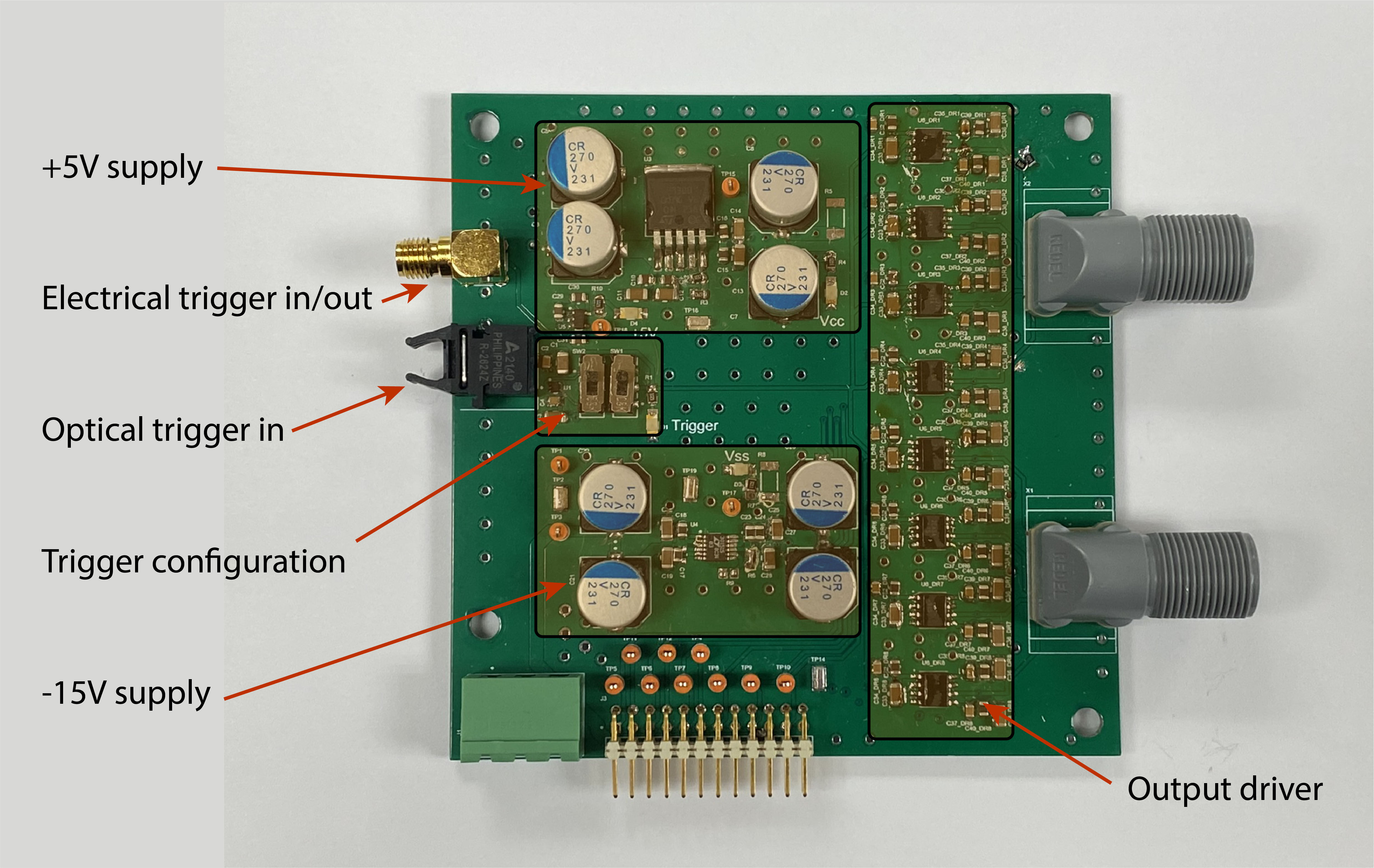
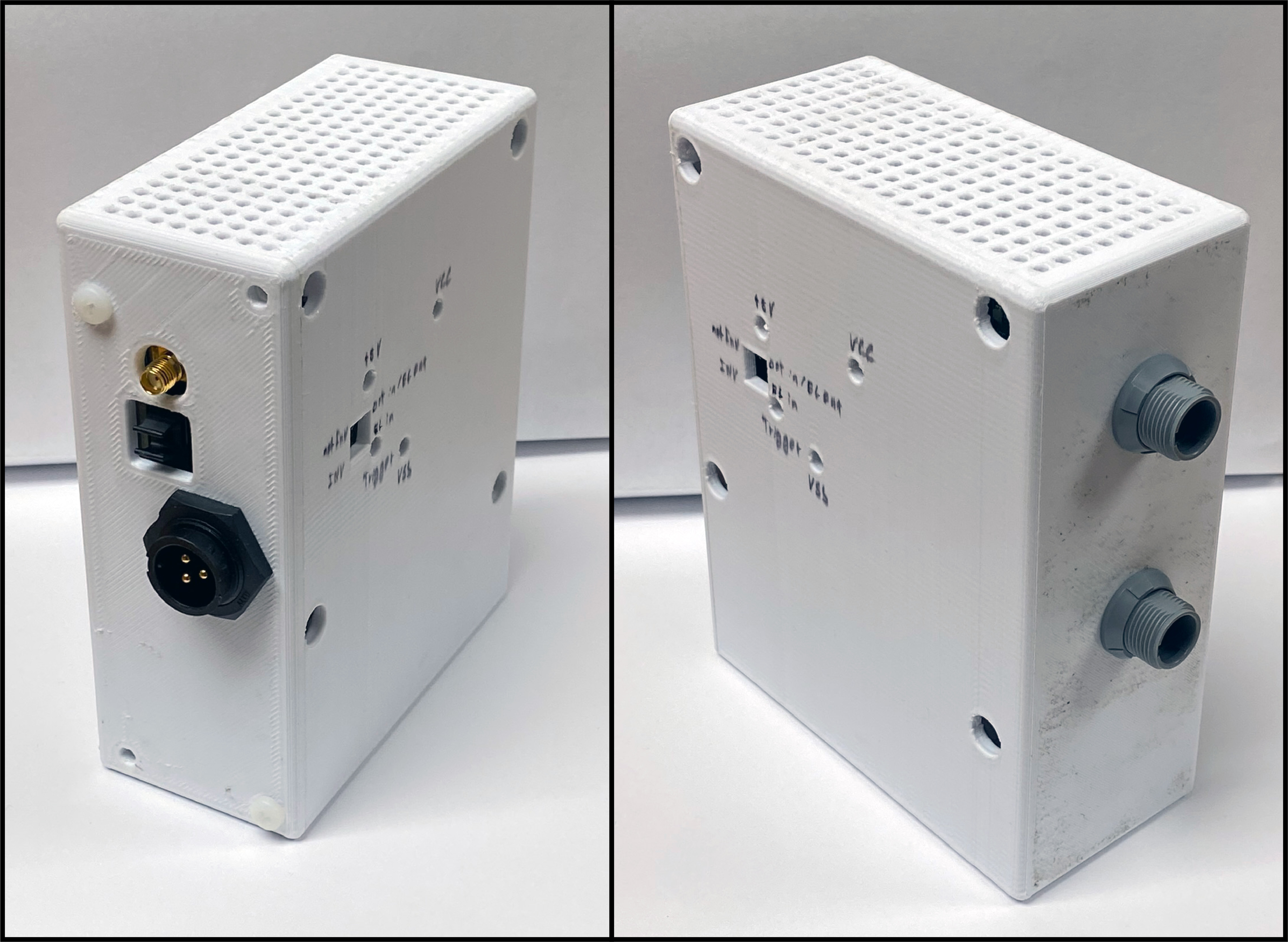
To achieve the PIN diode bias switching, a Maxim Integrated MAX22702 “Isolated Gate Driver”[16] was selected. Although no electrical isolation is required for switching PIN diodes, the isolation feature can be used for level shifting. The chip’s isolation is implemented as a capacitive gap which is compatible with B0 background fields found in-bore. Further, this chip can handle a peak of 4A positive current and 5.7A negative current. The tolerable average current is in the three-digit milliamp range, which is well in line with the needs of PIN diodes.A simplified schematic of the implemented driver is shown in Fig. 1. The design features both an optical and electrical interface. Eight driver chips were deployed on a 4-layer FR4 PCB, shown in Fig. 2, providing eight synchronously switching but otherwise electrically independent channels. The board was packaged into a 3D-printed housing and connectorized with plastic connectors and sockets.
On the bench, the rise and fall times and propagation delay were measured with the electrical trigger interface active. The data was collected with a Tektronix DPO 4104 5GSPS 500MHz BW oscilloscope. Measurements were performed with no load connected to the driver's output or a TR switch connected. Total idle power consumption was measured with an R&S NGE100 power supply.
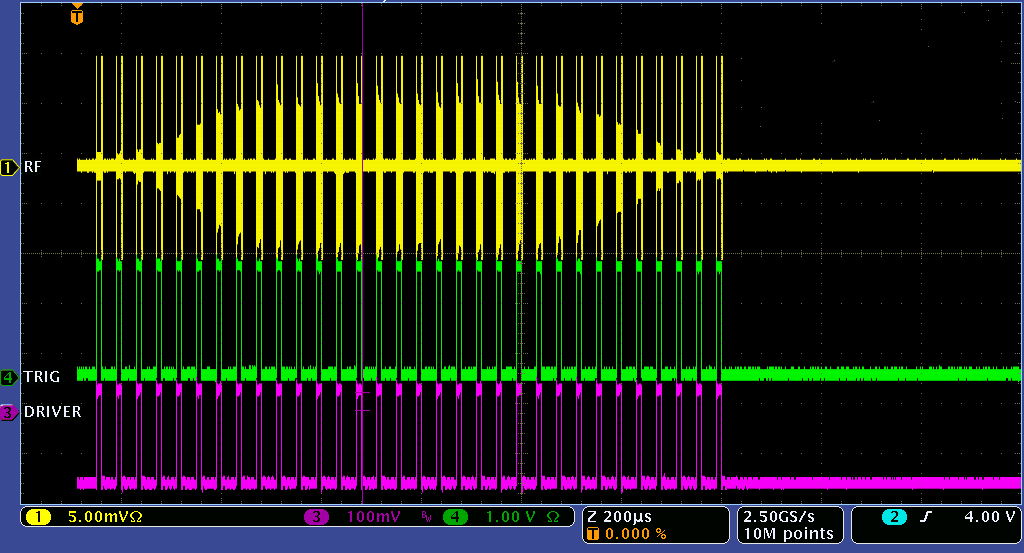
The driver was tested in-bore in a 10.5T MR system interfaced with a Siemens console where a SWIFT sequence was performed, and the voltages on the driver output, the trigger line, and the RF line were monitored.
Results
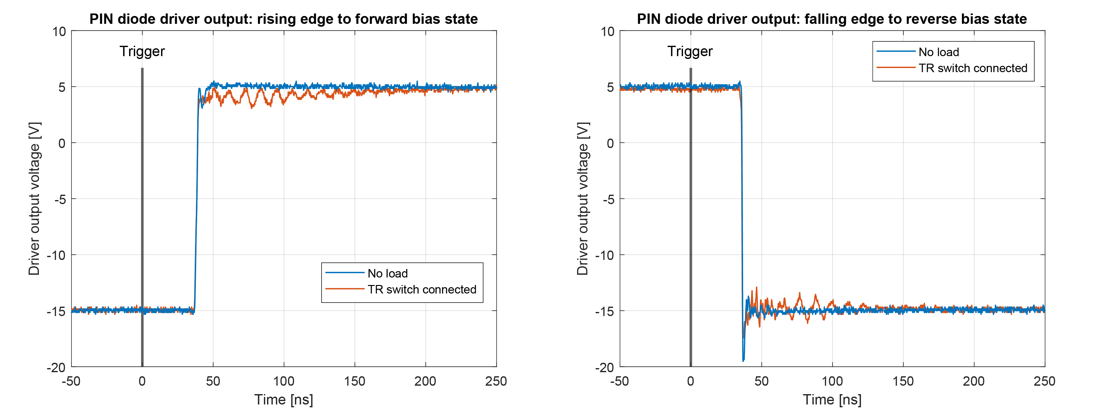
In Fig. 4, the output of the PIN diode driver is shown when switching from one bias state to the other. The rise time towards the forward bias state was measured to be 2.8ns with a TR switch connected, and 2.4ns with no load. The propagation delay was measured as 37.2ns in both cases. The fall time when switching towards the reverse bias state was measured to be 1.8ns with a TR switch connected, and 0.8ns with no load attached. The propagation delay was assessed as 34.6ns with a TR switch, and 35.8ns without a load. The idle power was measured as 0.62W on the positive input rail (7V, 89mA), and 0.61W on the negative input rail (-17V, 36mA).In Fig. 5, the monitoring voltages from the SWIFT sequence are shown. No anomalies could be detected, hinting at unimpeded PIN driver operation in-bore.
Discussion and conclusion
The presented PIN diode driver was shown to switch rapidly with only a few nanoseconds of rise and fall time. Further, the propagation delay, which was measured to be around 35ns, is also very low, and could be further calibrated out by trigger preemphasis. However, most certainly, the limiting factor in overall RF system switching time is now not limited by the driver but the PIN diode and its interfacing circuitry. Therefore to achieve faster RF system switching time, the optimization of the RF topology, component selection, and RF block circuits should yield the most significant gains.The observed ringing on the driver output with a TR switching connection could be avoided by matching the impedances of the transmission line, TR switch biasing input, and driver output. This matching would only be necessary for the frequencies with a wavelength on the same order or shorter than the PIN diode driver lines.
In conclusion, the presented PIN diode driver presents a plug-and-play solution for bench testing of switching RF hardware and in-bore MR experiments wherever PIN diodes are used. The driver is versatile in the interfacing and provides a simple single-chip solution making it easy to implement and of significant value for the interested MR engineering community.
Acknowledgements
No acknowledgement found.References
[1] Doherty, W. & Joos, R. The PIN diode circuit designers’ handbook. Microsemi Corporation 1, 1-137 (1998).
[2] Brunner, D. O. et al. Symmetrically biased T/R switches for NMR and MRI with microsecond dead time. Journal of Magnetic Resonance 263, 147-155, doi:https://doi.org/10.1016/j.jmr.2015.12.016 (2016).
[3] Lagore, R. L. et al. Fast transmit/receive switch for SWIFT imaging at 7T. Proc. Intl. Soc. Mag. Reson. Med. 27, 0573 (2019).
[4] Thapa, B., Kaggie, J., Sapkota, N., Frank, D. & Jeong, E.-K. Design and Development of a General-Purpose Transmit/Receive (T/R) Switch for 3T MRI, Compatible for a Linear, Quadrature and Double-Tuned RF Coil. Concepts in Magnetic Resonance Part B: Magnetic Resonance Engineering 46B, 56-65, doi:https://doi.org/10.1002/cmr.b.21321 (2016).
[5] Ronald D. Watkins, R. H. C., William E. Doherty. 298MHz Micro Miniature 2KW Transmit Receive Switch for 7.0 Tesla TR Arrays. Proc. Intl. Soc. Mag. Reson. Med. 20 (2012).
[6] Hafner, S. Fast imaging in liquids and solids with the Back-projection Low Angle ShoT (BLAST) technique. Magnetic Resonance Imaging 12, 1047-1051, doi:https://doi.org/10.1016/0730-725X(94)91236-P (1994).
[7] Madio, D. P. & Lowe, I. J. Ultra-fast imaging using low flip angles and fids. Magnetic Resonance in Medicine 34, 525-529, doi:https://doi.org/10.1002/mrm.1910340407 (1995).
[8] Wu, Y. et al. Water- and fat-suppressed proton projection MRI (WASPI) of rat femur bone. Magnetic Resonance in Medicine 57, 554-567, doi:10.1002/mrm.21174 (2007).
[9] Weiger, M. & Pruessmann, K. P. MRI with Zero Echo Time. Encyclopedia of Magnetic Resonance, doi:10.1002/9780470034590.emrstm1292 (2012).
[10] Grodzki, D. M., Jakob, P. M. & Heismann, B. Ultrashort echo time imaging using pointwise encoding time reduction with radial acquisition (PETRA). Magnetic Resonance in Medicine 67, 510-518, doi:https://doi.org/10.1002/mrm.23017 (2012).
[11] Idiyatullin, D., Corum, C., Park, J.-Y. & Garwood, M. Fast and quiet MRI using a swept radiofrequency. Journal of Magnetic Resonance 181, 342-349, doi:https://doi.org/10.1016/j.jmr.2006.05.014 (2006).
[12] Idiyatullin, D., Corum, C., Moeller, S. & Garwood, M. Gapped pulses for frequency-swept MRI. Journal of Magnetic Resonance 193, 267-273, doi:https://doi.org/10.1016/j.jmr.2008.05.009 (2008).
[13] Corum, C. A., Idiyatullin, D., Snyder, C. J. & Garwood, M. Gap cycling for SWIFT. Magnetic Resonance in Medicine 73, 677-682, doi:https://doi.org/10.1002/mrm.25141 (2015).
[14] Johansen, D. H., Albannay, M. M., Petersen, J. R., Zhurbenko, V. & Ardenkjær-Larsen, J. H. PIN diode driver for NMR and MRI. Journal of Magnetic Resonance 300, 114-119, doi:https://doi.org/10.1016/j.jmr.2019.01.017 (2019).
[15] Christoph Michael Schildknecht, M. W., Romain Froidevaux, and Klaas Paul Pruessmann. Rapid high power transmit-receive switching using a timed cascade of PIN diodes. Proc. Intl. Soc. Mag. Reson. Med. 29, 1411 (2021).
[16] Integrated, M. MAX22702E Datasheet, <https://datasheets.maximintegrated.com/en/ds/MAX22700D-MAX22702E.pdf> (2022).
Figures