4547
Monitoring performance of a GaN HEMT switch across different magnetic field strengths for implementation of On-Coil Tx Amplifiers
Brett Setera1,2, Aristos Christou2, and Natalia Gudino1
1Laboratory of Functional and Molecular Imaging, National Institutes of Health, Bethesda, MD, United States, 2Department of Materials Science & Engineering, University of Maryland, College Park, MD, United States
1Laboratory of Functional and Molecular Imaging, National Institutes of Health, Bethesda, MD, United States, 2Department of Materials Science & Engineering, University of Maryland, College Park, MD, United States
Synopsis
Keywords: New Devices, New Devices, Radiofrequency Technology
We present a method for monitoring multiple GaN HEMT device signals at different orientations with B0 during RF switching to determine possible magnetic field impacts on device performance and assist the development of an optimized GaN based device for on-coil amplification. Reduction in output current with increased magnetic field strength were not detected and device orientation did not impact signal amplitude.Introduction
On-coil RF transmit amplification provides several improvements for parallel transmit (pTx) systems at high and ultra-high field by reducing cabling restrictions and coupling, reducing cable losses, and allowing for more efficient and reliable power monitoring1–3. The on-coil pTx amplification system requires the power switch to perform high frequency switching while inside the strong magnetic field. Gallium Nitride high electron mobility transistors (GaN HEMTs) possess unique properties that make them good candidates as power switches in on-coil RF transmit amplifiers, and they have been successfully implemented for on-coil amplification at 300MHz (7T) and 500MHz (11.7T)3. Currently, however, no data is available for how commercial GaN devices are impacted by exposure to high and ultra-high fields during RF switching. Magnetic field impacts on Silicon-based JFET transconductance were previously investigated under DC bias and showed that increased field strength results in reduced current with a strong dependence on orientation between the device and B0 as dictated by the Lorentz force4. To determine possible impacts on device performance, we present a method for monitoring multiple GaN HEMT device signals at two different orientations with the static magnetic field during RF switching. This research will assist in the development of an optimized GaN device for on-coil RF amplification at high and ultra-high field MRI.Methods
A simple switching block (Fig. 1a) was built using a commercial enhancement-mode GaN HEMT (eGaN, EPC Corporation, EPC8009) directly connected to a Tx surface loop tuned to 297.2 MHz. To minimize cabling mechanical restrictions and avoid crosstalk, an optical digital connection transmitted the RF signal to the test circuit with the device under test (DUT), and a single coaxial connection transmitted one sensor signal at a time from the test circuit to an oscilloscope using a 4:1 multiplexer (ADG1204, Analog Devices Inc.). Earlier experiments determined that the B0 field has no measurable impact on the multiplexer. To avoid interference of possible B0 effects on electronic components other than the DUT, test circuit simplification was prioritized. A basic Class E design ensured a minimization of components and allowed testing a single device switch with simple control. The circuit was loaded with a phantom simulating average brain tissue placed above the transmit surface loop. To determine the impacts of orientation between the FET and B0, two EPC devices were assembled on the test circuit to be configured as the single switch (Fig 1a, inset) and compare its performance when placed parallel and perpendicularly to the field. The drain was biased at 10V and, differently from a switch-mode amplifier topology as used in on-coil amplification, the gate was biased at the threshold voltage with a 2.3V pulse (2 % duty cycle). This configuration avoids the need for a driver circuit which would contain other electronic components that would have to be included in the magnetic field performance analysis. The test circuit was placed inside the bore of 7T MRI Scanner (Siemens, Erlangen) (Fig. 1b) and data points were acquired while locating the patient table at selected static field contours provided by the magnet’s manufacturer. Due to the mobility requirements of the setup, multiple measurements were taken to avoid error caused by shifting cables (multiplexer coaxial output and DC connections) when moving the patient table/test circuit through the field gradient.Results
The simple test circuit successfully switched the DUT at 297.2 MHz and the 4:1 multiplexer was able to switch between signals, including the output current (Fig. 2b) and a pulsed gate bias signal (Fig. 2a). The B1 field strength through the tuned surface loop was 1.5 μT as measured via calibrated probe. Output current was analyzed using the fast Fourier transform signal by comparing the peak amplitude at 297.2 MHz at each field strength (Fig. 3). Figure 3 shows that reduction in output current at increased field strengths was not detected and that device orientation had no impact on signal amplitude. Differences in peak amplitude between parallel and perpendicularly oriented devices were caused by switching via jumper between devices and are not indicative of any B0 effects. The largest standard deviation of peak amplitude was 0.08 dBm at both 0.2T and 5T for the perpendicularly oriented device. Average standard deviation across all field strengths was 0.05 dBm for perpendicular orientation and 0.03 dBm for parallel orientation. The 3rd harmonic peak average standard deviation across all fields was 0.26 dBm for perpendicular orientation and 0.29 dBm for parallel orientation.Discussion
Understanding magnetic field effects on GaN HEMT power switches is imperative for the development of devices optimized for use in on-coil pTx amplification as B0 is consistently being increased to improve imaging quality. Future work investigating two more device orientations in the magnetic field and the monitoring of multiple device signals during switching is currently under development. Signals to be monitored include gate voltage, gate current, drain voltage, and drain current. Using these four signals, device parameters such as parasitic capacitances, gate charge, transconductance and on-resistance can be extracted at varying magnetic field strengths to determine any possible field effects. This device level analysis will determine if magnetic field effects must be taken into consideration during the development of an optimized GaN HEMT power switch.Acknowledgements
University of Maryland, College Park; LFMI, NIH; Section on Instrumentation at NIMH, NIHReferences
1. Gudino, N., de Zwart, J. A., van Gelderen, P. & Duyn, J. H. ISMRM 2017 Abstract 0758.
2. Gudino, N. et al. Optically controlled on-coil amplifier with RF monitoring feedback. Magn. Reson. Med. 79, 2833–2841 (2018).
3. Gudino, N. et al. Optically controlled switch-mode current-source amplifiers for on-coil implementation in high-field parallel transmission. Magn. Reson. Med. 76, 340–349 (2016).
4. Bodart, J. R. et al. The effect of high magnetic fields on junction field effect transistor device performance. Rev. Sci. Instrum. 69, 319–320 (1998).
Figures
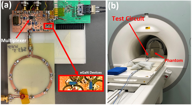
Fig 1. Photos of device monitoring setup
(a) test circuit with fiber optic connection and transmit coil, inset showing
transversely oriented eGaN devices. Fiber optic
connection shown on top right and surface loop on bottom left. Circuit
components were mounted to a block for increased mechanical stability. (b) Setup
inside the 7T scanner with phantom on transmit coil.
Sandbags were placed over cables to prevent the test circuit from altering its
position when moving patient bed through the field gradient.
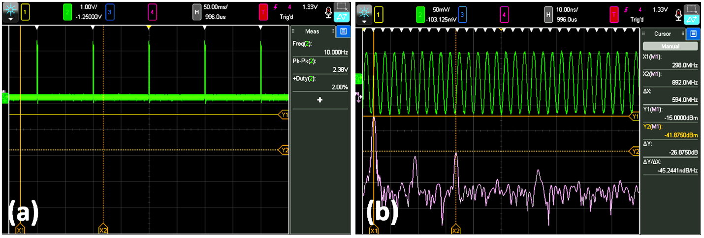
Fig 2. Oscilloscope
images confirming successful signal switching at 7T through the 4:1 multiplexer
(a) pulsed gate bias signal (b) RF output current and FFT.

Fig 3. Peak amplitude at 297.2
MHz from FFT signal at varying field strength with device parallel and perpendicularly oriented with B0. Differences in peak amplitude
between parallel and perpendicular orientation are due to switching the output
signal between devices via jumper and are not indicative of B0
effects.
DOI: https://doi.org/10.58530/2023/4547