3867
A Balanced RF Switch for Ultra-Wideband System with Microsecond Dead Time1Shanghai Key Laboratory of Magnetic Resonance, School of Physics and Electronic Science, East China Normal University, shanghai, China, 2Athinoula A. Martinos Center for Biomedical Imaging, Department of Radiology, Massachusetts General Hospital, Charlestown, MA, United States, 3John A. Paulson School of Engineering and Applied Sciences, Harvard University, Cambridge, MA, United States
Synopsis
This work demonstrated a fully balanced strcture of wideband RF switch. The switch utilizes PIN diodes to form two balanced paths which transmit the RF signals in common mode and the drive signal of PIN diode in differential mode.The common-mode choke can be used to block AC signal and feed DC bias. It can also be used to suppress the transient voltage due to the drive signal. The switch achieved low insertion loss and high isolation within a bandwidth between 10MHz-100MHz. The switch also suppressed the transient voltage to less than 3.3mV with a very short dead time.
Purpose
Non-resonance circuits have been used in ultra-wideband low-frequency magnetic resonance systems which operated in the 0.1-3 MHz1. RF switch, which works as the first stage of RF channel and controls the RF path, is one of the important factors to determine the performance of the system. To expand the operating frequency of RF switch for various applications such as multi-nuclei acquisitions and wideband NMR, a fully balanced RF switch was designed to work in ultra-wide frequency range with excellent RF characteristics in this study.Methods
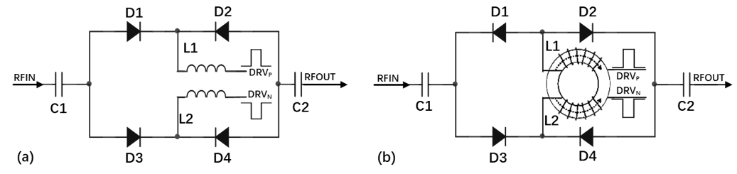
Balanced RF switchA novel balanced topology of RF switch was proposed in this study. As shown in Fig. 1a, the up path (D1, D2, L1) and down path (D3, D4, L2) are formed as two paralleled RF channels with back-to-back structure. When D1 to D4 are in forward-biased, they will appear as low impedance to RF signal. When the polarities of bias voltage are reversed, the PIN diodes appear as an open circuit or large resistance with some associated reverse bias capacitance of the series diodes2. The two RF paths placed in a balanced fashion enables an important feature that the RF signal in each path is symmetrically and the bias voltages at DRVP and DRVN are applied in a differential mode. This feature allows the inductors (L1, L3) which reduce the RF leakage to be replaced by a common-mode (CM) choke (Fig. 1b).The CM choke exhibits a very low resistance and inductance to the differential bias voltage to allow rapid switching, signals to be provided to the PIN diodes without high excess voltage spikes being produced across the choke3.
Pin diode driver
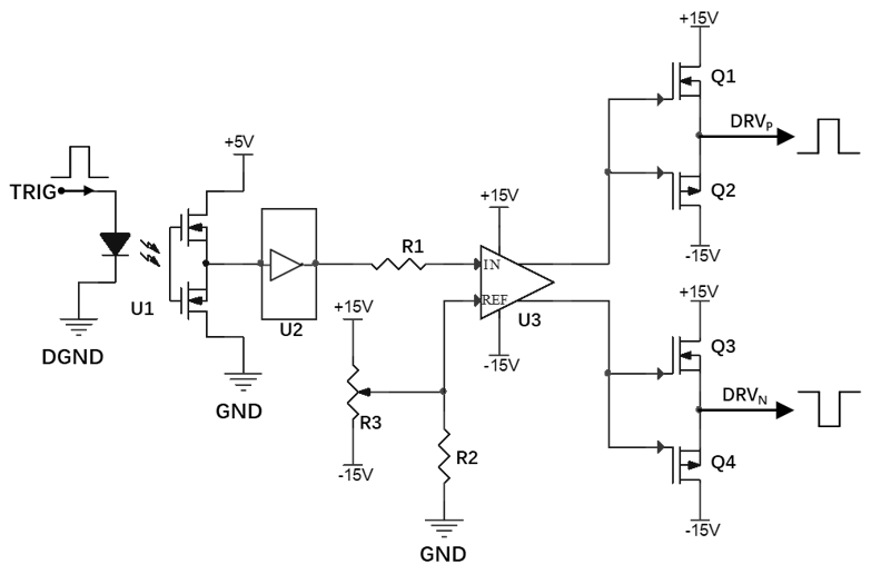
Fig. 2 shows the schematic diagram of differential drive circuit for balanced PIN diode. The trigger signal is input from the TRIG port. U1 is a high-speed optical coupler which is used for eliminating the ground loop noise, particular important if the trigger signal is fed through a long cable. U2 is a set of logic circuits which is used for 0~512μs delay and shaping the waveform of optical coupler’s output. U3 is a differential amplifier for the driver stage and it is used to convert the single-end signal into differential mode. The driver stage consists of a set of four MOSFET (Q1, Q2, Q3, and Q4) arranged in a circuit known as an H-bridge or full bridge4.
Results
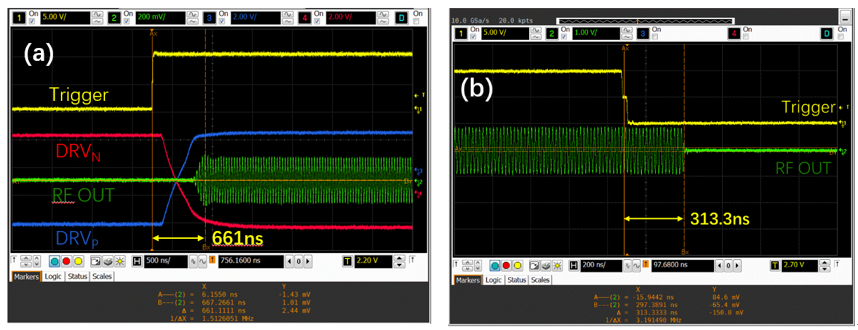
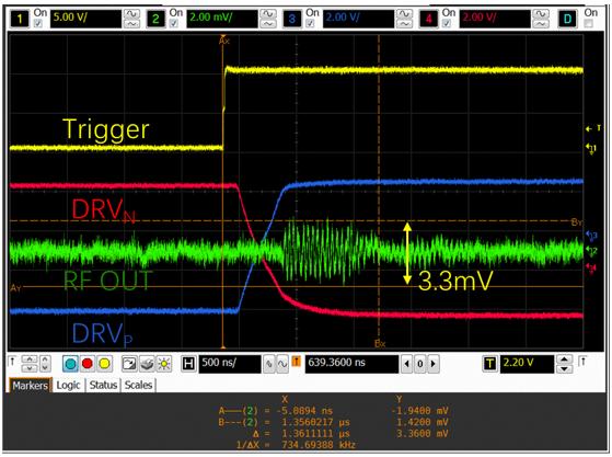
To evaluate the RF switch performance, the insertion loss and isolation of the RF switch were measured with frequency from 10MHz-100MHz by a network analyzer (4396B, Agilent, Inc., Santa Clara, CA). The results showed that good impedance matching conditions could be achieved. The insertion loss at ON state was less than 1dB and the isolation of the switch at OFF state was greater than 64dB. Fig. 3a&b show the switching time of the RF switch. As shown in Fig. 3a&b, the turn-on time is about 661ns and the turn-off time is about 331.3ns. Fig. 4 shows the transient response of the RF switch and the transient voltage were limited to only 3.3mV as a result of the common-mode choke.Discussion
This work demonstrated a new topology of RF switch for ultra-wideband system with a high power transmission and high sensitivity reception. The balanced RF paths of the switch, which utilized the merit of CM choke to cancel the inductance effect and the back-to-back structure of PIN diode with proper drive method, could inherently provide relative high power handling capacities with very short dead time.Acknowledgements
The authors are grateful to Liping Xu for valuable discussions in hardware development.References
1. Hopper T, Mandal S, Cory D, et al. Low-frequency NMR with a non-resonant circuit. Journal of Magnetic Resonance, 2011, 210: 69-742.
2. Medina-Plata, M. A., G. Leija-Hernandez, and L. A. Iturri-Hinojosa. Performance analysis of PIN diodes in microwave switches. Journal of Vectorial Relativity, 2009, JVR, 4(4) : 110-116.3.
3. Brunner DO, Furrer L, Weiger M, et al. Symmetrically biased T/R switches for NMR and MRI with microsecond dead time. Journal of Magnetic Resonance, 2016, 263: 147-1554.
4. Johansen DH, Albannay MM, Petersen JR, et al. PIN diode driver for NMR and MRI. Journal of Magnetic Resonance, 2019, 300: 114-119
Figures