3840
Effect of doping on the dynamic nuclear polarization of porous silicon nanoparticles1Department of Applied Physics, University of Eastern Finland, Kuopio, Finland, 2Institute for Biomedical Engineering, ETH Zurich, Zurich, Switzerland, 3Laboratory of Physical Chemistry, ETH Zurich, Zurich, Switzerland, 4A.I. Virtanen Institute, University of Eastern Finland, Kuopio, Finland
Synopsis
Porous Si nanoparticles (NPs) with different doping degree were prepared using low-load metal assisted catalytic etching and subjected to dynamic nuclear polarization at 3.4 T and 6.7 T. Thermal oxidation of Si was applied to form paramagnetic centers of dangling bond type in Si/SiO2 interface, which were used to polarize 29Si nuclei. The doping significantly affected the gained polarization and buildup times: high doping degree generally led to lower and faster polarization compared to the low doping. On the other hand, slight p-type or n-type doping was necessary to achieve the highest polarization of about 11 %.
Introduction
In the past decade there has been a substantial effort to develop Si microparticles1 and nanoparticles2,3 (NPs) as an alternative to 13C labeled molecules for hyperpolarized magnetic resonance imaging (MRI). The objective has been to develop imaging agents (IAs) with long relaxation time and depolarization times of about 40 min have been reported.1–3However, there has been little effort to systematically understand the effect of Si structural parameters on the polarization, which is required for the design of Si NP based IAs. Herein, porous Si NPs were prepared by a controlled reproducible top-down fabrication approach that allows the control of the density of doping atoms, particle size and structure as well as surface properties.
Materials and Methods
Single crystal Si wafers (Okmetic Oy) of varied doping (p-type and n-type with specific resistivities ρ of 0.01-5000 Ω∙cm) were milled using a planetary ball mill (Fritsch Pluverisette 7), washed in ~3% H2O2 (Acros Organics), filtered through 10 µm Whatman® paper and dried to obtain bulk microparticles of 10-25 µm. The microparticles were then subjected to low-load metal (Au) assisted catalytic etching (LL-MACE)4,5 to produce porous microparticles with high specific surface area. Porous microparticles were then thermally oxidized at 300 ºC for 2 h and ball milled again to obtain porous Si NPs of ~150 nm. About 100 mg of Si NPs were dried and packed into a plastic container that was then placed into a DNP spectrometer.To study DNP, two different spectrometers were used: SpinAligner (Polarize ApS) operating at 6.7 T and 1.4 K, and a home-built setup based on the OpenCore NMR operating at 3.4 T and 3.4 K. Sweep spectra and polarization buildups were acquired with chain-saw modulation of microwave frequency with bandwidth of about 200 MHz.3 Acquired FIDs were analyzed with custom MATLAB® scripts; each FID was Fourier transformed, fitted with Voigt function which was then integrated to obtain the NMR peak area. Peak areas were normalized to the sample mass and recalculated to NMR signal enhancement and polarization degree using the thermal polarization data. The buildup data was fitted with one or two exponential functions at 6.7 T and 3.4 T, respectively.
Results and Discussion
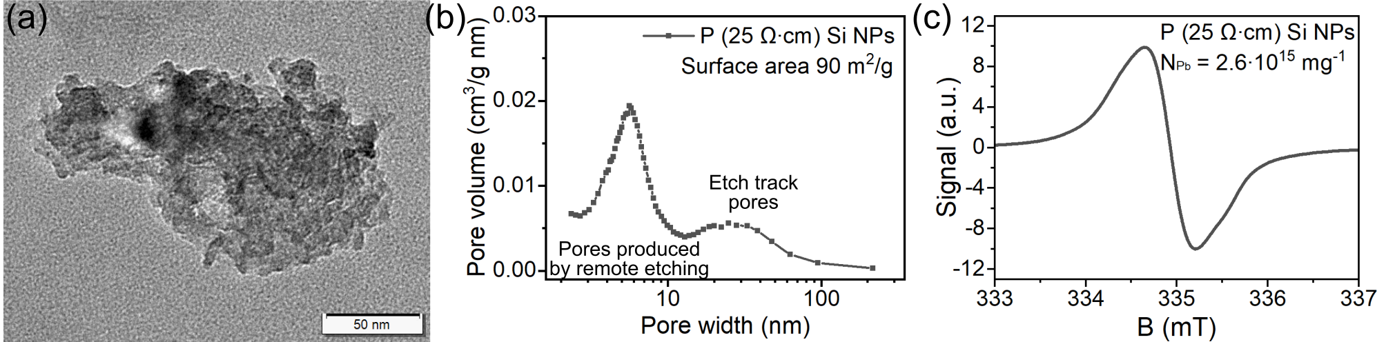
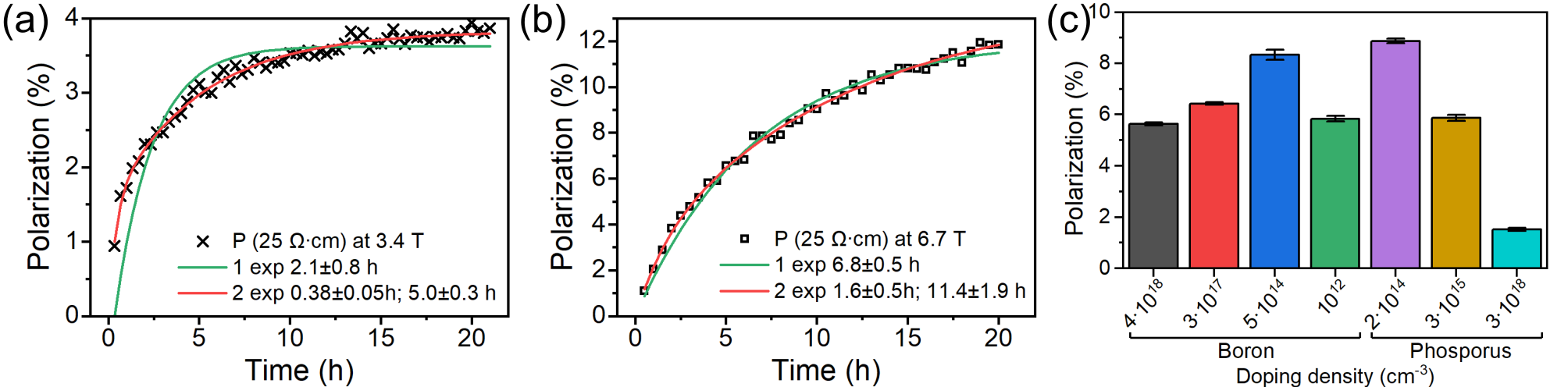
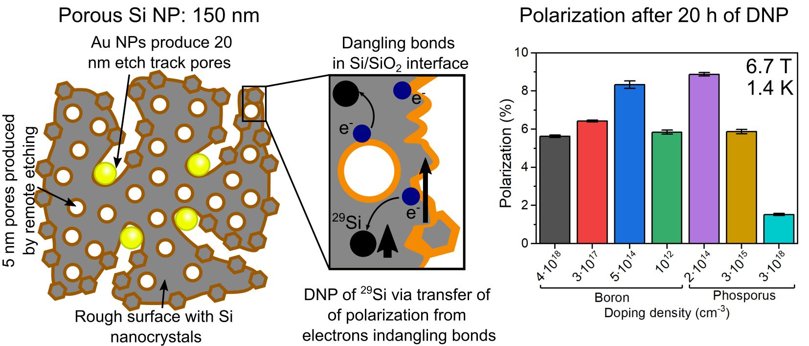
LL-MACE is a recently developed method that makes it possible to porosify Si of different grades – a prerequisite for high surface area and correspondingly high number of paramagnetic centers needed for DNP. Typical Si NPs fractured by ball milling of porous microparticles have an average size of 150 nm and irregular shape (Figure 1a). Pore network consists of larger etch track pores produced by metal NP movement and remote etching of etch track pore walls (Figure 1b).4,5 Thermal oxidation resulted in growth of thin oxide layer on the Si surfaces,6 which leads to the formation of Pb centers in the Si/SiO2 interface. Pb centers are paramagnetic defects of Si dangling bond type originating from the lattice mismatch between Si and SiO2.7 A typical electron paramagnetic resonance spectrum of Pb centers in p-type Si NPs (ρ = 25 Ω∙cm) and the corresponding number of Pb centers NPb is shown in Figure 1c.Polarization buildup of p-type Si NPs is depicted on Figure 2a at 3.4 K and 3.4 T and on Figure 2b at 1.4 K and 6.7 T. Due to higher thermal polarization of electrons the polarization of 29Si nuclei is higher at 6.7 T than at 3.4 T for the same Si doping. The highest achieved polarization was about 11 %. It was found that buildup dynamics differ at 3.4 T and at 6.7 T. At 3.4 T the buildup is significantly better described with a DE fit compared to 6.7 T; at high field the DE fit gives high errors to the fitted time parameters for all the Si doping levels studied (data not shown). Note, that analysis of R2 cannot be adequately performed for nonlinear fits8 and thus R2 values are not presented here.
Figure 2c compares the maximum polarization achieved after 20 h of DNP for different Si types. Three prominent results are: (1) slight doping of either p or n type is needed to achieve the highest polarization levels (blue and magenta bars compared to green bar); (2) moderately doped Si NPs of p and n type perform similarly; (3) when Si becomes metallic in case of highly phosphorus doped Si NPs (cyan bar) the efficiency of DNP decreases significantly.
Conclusions
Porous Si NPs with high surface area were produced from crystalline Si of different purity with a controlled etching technique. The high surface area was necessary to form enough paramagnetic Pb centers that were acting as the polarized source for DNP of 29Si nuclei. Performing dynamic nuclear polarization at 3.4 and 6.7 T, the effect of doping and magnitude of magnetic field was studied to obtain a high polarization level of about 11 %.Acknowledgements
Funding is provided by Academy of Finland grants #314551, #332006, and #331371. The microscopy studies were performed using the facilities of SIB Labs, Laboratory of Microscopy at the University of Eastern Finland. Silicon was provided by Elkem Silicon Materials and Okmetic.References
(1) Cassidy, M. C.; Chan, H. R.; Ross, B. D.; Bhattacharya, P. K.; Marcus, C. M. In Vivo Magnetic Resonance Imaging of Hyperpolarized Silicon Particles. Nat. Nanotechnol. 2013, 8, 363–368.
(2) Atkins, T. M.; Cassidy, M. C.; Lee, M.; Ganguly, S.; Marcus, C. M.; Kauzlarich, S. M. Synthesis of Long-T1 Silicon Nanoparticles for Hyperpolarized 29Si Magnetic Resonance Imaging. ACS Nano 2013, 7, 1609–1617.
(3) Kwiatkowski, G.; Polyhach, Y.; Jähnig, F.; Shiroka, T.; Starsich, F. H. L.; Ernst, M.; Kozerke, S. Exploiting Endogenous Surface Defects for Dynamic Nuclear Polarization of Silicon Micro- and Nanoparticles. J. Phys. Chem. C 2018, 122, 25668–25680.
(4) Tamarov, K.; Swanson, J. D.; Unger, B. A.; Kolasinski, K. W.; Ernst, A. T.; Aindow, M.; Lehto, V.-P.; Riikonen, J. Controlling the Nature of Etched Si Nanostructures: High-versus Low-Load Metal-Assisted Catalytic Etching (MACE) of Si Powders. ACS Appl. Mater. Interfaces 2020, 12.
(5) Tamarov, K.; Kiviluoto, R.; Swanson, J. D.; Unger, B. A.; Ernst, A. T.; Aindow, M.; Riikonen, J.; Lehto, V.-P.; Kolasinski, K. W. Low-Load Metal-Assisted Catalytic Etching Produces Scalable Porosity in Si Powders. ACS Appl. Mater. Interfaces 2020, 12, 48969–48981.
(6) Riikonen, J.; Salomäki, M.; Van Wonderen, J.; Kemell, M.; Xu, W.; Korhonen, O.; Ritala, M.; MacMillan, F.; Salonen, J.; Lehto, V. P. Surface Chemistry, Reactivity, and Pore Structure of Porous Silicon Oxidized by Various Methods. Langmuir 2012, 28, 10573–10583.
(7) Helms, C. R.; Poindexter, E. H. The Silicon-Silicon Dioxide System: Its Microstructure and Imperfections. Reports Prog. Phys. 1994, 57, 791–852.
(8) Spiess, A.-N.; Neumeyer, N. An Evaluation of R2 as an Inadequate Measure for Nonlinear Models in Pharmacological and Biochemical Research: A Monte Carlo Approach. BMC Pharmacol. 2010 101 2010, 10, 1–11.
Figures