2260
Studying the influence of cryogenic cooling and B0 alignment on Si PIN diode operation in active decoupling circuits1Department of Electrical Engineering, Technical University of Denmark, Kongens Lyngby, Denmark, 2Department of Health Technology, Technical University of Denmark, Kongens Lyngby, Denmark
Synopsis
Si diodes can require elevated forward bias voltage to achieve sufficient forward bias current when they are placed in a strong static magnetic field B0 at cryogenic temperatures. This may disrupt active decoupling circuit operation in cryogenic MRI coils. Diodes may still operate if aligned in a certain way with the B0 field, which is studied in this work.
Introduction
In MR, semiconductor devices operate under strong static magnetic field B0, most commonly 1.5 T and 3 T. The Hall Effect has been reported to affect GaAs FETs1, for which attention must be paid to transistors’ orientation. Here, the effect on Si diode orientation at -160°C and 3 T is studied. It is shown that for some diodes traditionally used in MRI, this effect leads to the active decoupling circuit failing to turn ON in cryogenic cooled coil2,3.Methods
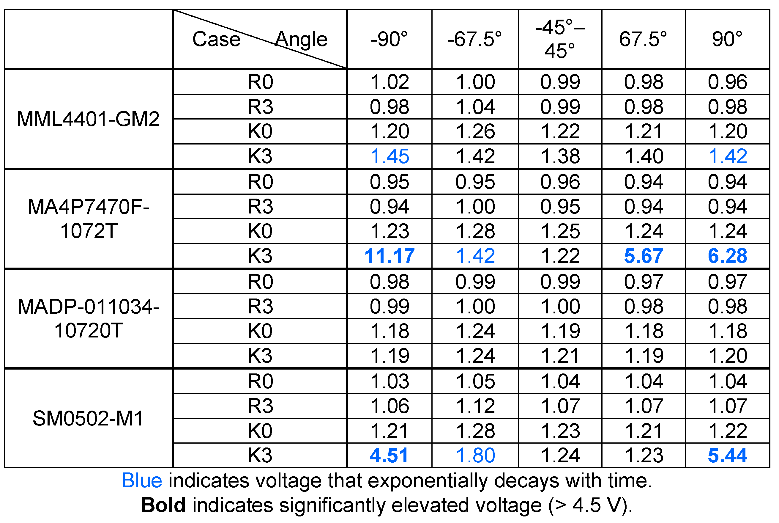
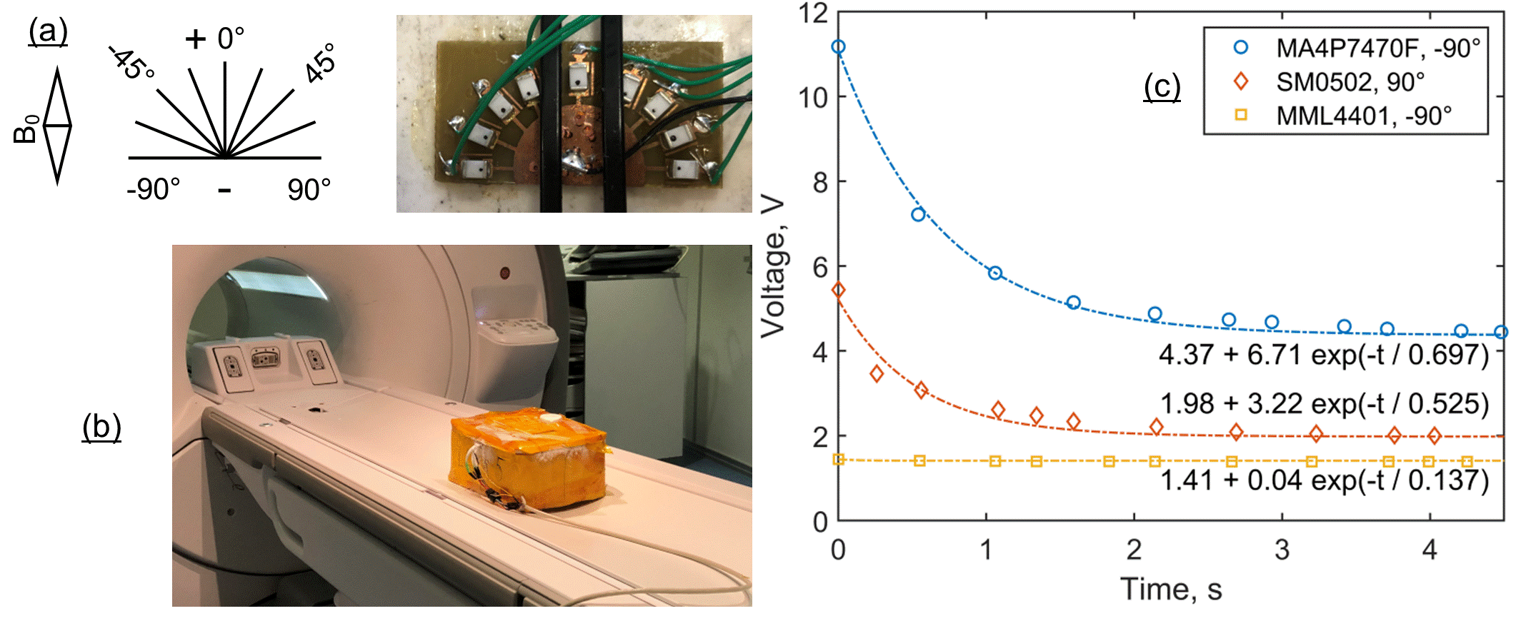
To study the effect of Si diode orientation on forward bias, four types of MR-compatible Si diodes are used: MML4401-GM2 from Microsemi Corp. (Aliso Viejo, CA, USA), and MA4P7470F-1072T, MADP-011034-10720T, SM0502-M1 from MACOM Inc. (Lowell, MA, USA). Each type of diodes are put at 9 angles in 22.5° step, as shown in Figure 2(a). The carrier printed circuit boards (PCBs) are mounted on a cryostat that cools the temperature to approx. -160°C (113 K). The cryostat is then put inside a clinical 3 T MR scanner (MR750, General Electric, US), so that the diodes intersect with B0 at angles of -90°, -67.5°, -45°, -22.5°, 0°, 22.5°, 45°, 67.5°, 90°. The experiment setup is shown in Figure 2(b).A DC power source (Aim-TTi-MX100TP, Cambridgeshire, UK) is used to forward bias diodes by 50 mA, the minimum ON-state current for active decoupling circuits allowed by the scanner. For MR safety, current is fed through a cable of 11 m from outside the scanning room. The corresponding forward bias voltages are taken to assess the influence of diode orientation in four study cases: room temperature without magnetic field (R0), room temperature in 3 T magnetic field (R3), cryogenic temperature without field (K0), and cryogenic temperature in 3 T field (K3).
Results
The voltages needed to forward bias diodes by 50 mA are listed in Figure 1. No effect of orientation is observed for diodes outside B0 or at room temperature. Moreover, not all Si diodes experience sharp voltage increase inside B0 around -160°C. At ±90° with B0, the diode MA4P7470F-1072T experiences the severest effect with forward voltage climbing to 11.17 V, followed by SM0502-M1 with 5.44 V, whereas little effect is observed for MADP-011034-10720T and MML4401-GM2. At ±67.5°, the effect of orientation dwindles but remains significant for MA4P7470F-1072T. Little or no voltage drop is observed for other angles or diode MADP-011034-10720T. The asymmetry of data at ±90° and ±67.5° results in part from placement error that accumulates when PCBs are mounted on the cryostat and the cryostat is put in the scanner.For MA4P7470F-1072T and SM0502-M1 at and near ±90°, the forward voltage drops exponentially while the forward bias current remains 50 mA, as shown in Figure 2(c). Feeble exponential decay of forward bias voltage is observed for MML4401-GM2. The fitted time constants are 697 ms, 525 ms and 137 ms for MA4P7470F-1072T, SM0502-M1 and MML4401-GM2, respectively. Steady-state voltage is 4.37 V, 1.98 V, and 1.41 V for MA4P7470F-1072T, SM0502-M1 and MML4401-GM2, respectively.
Discussion
The significant voltage increase appears only for diodes MA4P7470F-1072T and SM0502 and only at angles near ±90°. Nonetheless, if it happens, the forward bias voltage can rise by 9.9 V. Taking into account the time constant as high as 697 ms, it follows naturally that circuitry employing these diodes like active decoupling circuits can fail to be turned ON by an 8 V supply for merely 1 ms from scanners. Even if the voltage supply can last longer than the voltage decay, the 4.37 V steady-state voltage is still a high barrier. This will block ensuing scanning processes. Therefore, for builders of cryogenic coils, it is advisable to make sure that diodes to be used have no noticeable orientation effect or to put them parallel to B0.The effect of Si diode orientation may be attributed to the magnetoresistance effect, which comes on the scene when semiconductor devices are placed in a strong magnetic field. The strong magnetic field warps carriers’ paths inside Si crystals, incurring stronger carrier scattering and consequently higher device resistance, particularly when carrier mobility is high4, which is the case at -160°C, but not at room temperature4. Severity of the effect, as follows from the experiment results, differs among diodes.
The exponential voltage decay may reflect a transient process during which high power dissipation causes local temperature to rise, which alleviates the effect of diode orientation until a steady state is reached. Voltage decay is hardly visible for diodes that intersect with B0 at -45°–+45° at -160°C, outside magnetic field at -160°C, or at room temperature, suggesting the 11 m cable plays at most a minor role in contributing to the voltage decay.
Conclusion
At cryogenic temperature of -160°C, orientation of Si diodes has importance; when diodes intersect the B0 field at near 90°, device resistance can increase sharply, elevating the forward bias voltage and thereby blocking normal scanning processes. It is recommended that builders of cryogenic coils examine the orientation effect in advance, and place Si diodes parallel to B0 to avoid it if the effect exists.Acknowledgements
No acknowledgement found.References
1. Possanzini C, Boutelje M. Influence of magnetic field on preamplifiers using GaAs FET technology. Proc 16th Sci Meet Int Soc Magn Reson Med. 2008;Toronto:1123. /MyPathway2008/1123.
2. Wang W, Sánchez-Heredia JD, Zhurbenko V, Ardenkjær‐Larsen JH. Towards a cryogenic RF coil array for 13C human head imaging: first experience. In: Proceedings of the International Society for Magnetic Resonance in Medicine 29. ; 2021:2502.
3. Sánchez‐Heredia JD, Baron R, Hansen ESS, Laustsen C, Zhurbenko V, Ardenkjær‐Larsen JH. Autonomous cryogenic RF receive coil for 13C imaging of rodents at 3 T. Magn Reson Med. 2020;84(1):497-508. doi:10.1002/mrm.28113
4. Sze SM, Ng KK. Physics and Properties of Semiconductors—A Review. In: Physics of Semiconductor Devices. 3rd ed. John Wiley & Sons, Inc.; 2007:1–72.
Figures