Coil-Building Demonstration
1Institute for Medical Physics and Radiation Protection, TH Mittelhessen University of Applied Sciences (THM), Giessen, Germany
Synopsis
In this educational video, we describe the step-by-step procedure for constructing and tuning highly parallel array coils: (1) the layout of the array elements, (2) creating and tuning a single loop element, (3) estimating the coil quality factor, (4) adjusting the single loop and match circuit to optimize preamplifier decoupling and (5) active PIN diode detuning circuitry, (6) placing the neighboring elements to allow them to be efficiently constructed and inductively decoupled, (7) assembling the array, (8) decoupling the array elements from one another, (9) tune and match the coil elements, and (10) performing final bench tests
Introduction
In this educational video, we describe the step-by-step procedure which we have developed for constructing and tuning highly parallel array coils. We will describe an array geometry with coil overlaps to reduce nearest-neighbor decoupling, although the procedure becomes simpler if a gapped design is used (in which case there is no geometric overlap to optimize). If shared-capacitive decoupling is used, the procedure is also similar, with the adjustment of the shared capacitor replacing the geometric optimization. Additionally, we used a design, where the preamplifiers are mounted adjacent to each coil element to minimize losses between the inductive loop and the first stage of amplification. The close proximity between loop and preamplifier eliminates the need for a long cable between loop and preamplifier. In addition to reducing losses, this approach opens a new degree of freedom to match the coil’s impedance so that the load impedance seen by the preamplifier differs from the traditional 50 Ω. This load impedance must be matched to the load impedance ZNM required to operate the preamplifier at the lowest noise figure but can, in principle, be chosen based on preamplifier design considerations or to facilitate some aspect of the coil matching circuit. Choices other than the traditional 50 Ω complicate certain measurements, where it is necessary to temporarily transform the coil impedance to 50 Ω so that it can be connected to the port of a network analyzer (with 50 Ω system impedance). Nonetheless, we describe the construction procedure for this general case.1) Helmet Design
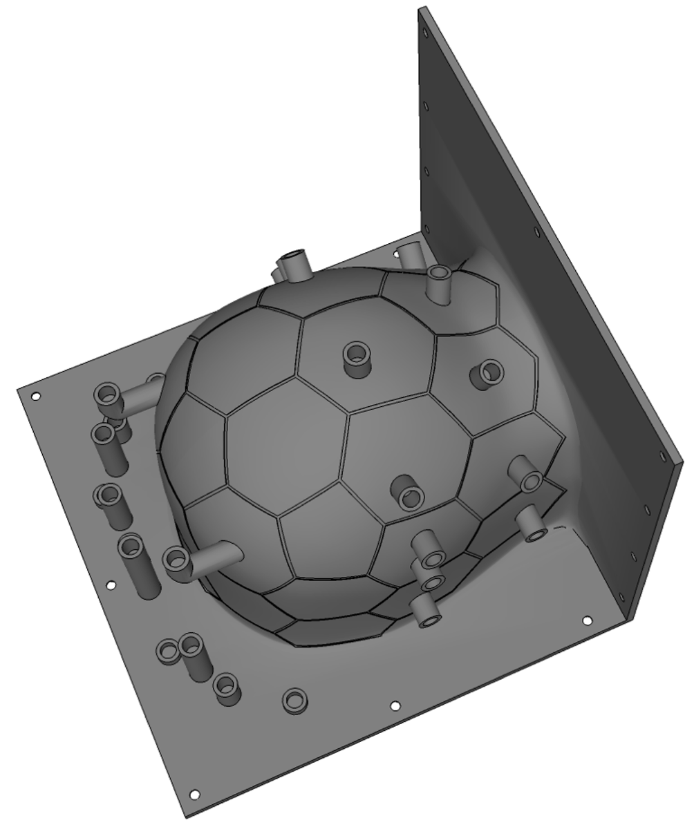
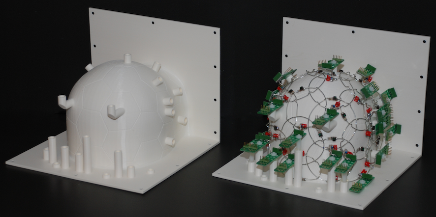
The helmet size was obtained from the surface contours of aligned 3D MRI scans. In our case we are going to build a coil for children. The helmet shape was taken by dilating the 95% contour to accommodate 3mm foam padding. Using a 3D CAD program, the helmet was designed as a deep posterior segment covering all but the face and forehead so the child can lie down into the posterior coil section. A separate “frontal paddle” is then positioned over the forehead. This configuration simplifies the need to mate the two segments and avoids a single helmet which comes down over the head. It maintains an open area over the eyes and face. This coil design is an example of a sized-matched array to be used for 1-year-old children [6]. The helmet model is shown in Figure 1. The geometric structure of the coil element layout (shown below) was engraved on the helmet as Section of the CAD design (Figure 1). Additionally, standoffs for the preamplifiers were included into the 3D design. We also constructed a size-matched head-shaped phantom derived from the statistical head surfaces. We placed this phantom in the tightly fitting coil array and used it for loading the coil during adjustments at the bench as well as test imaging acquisitions on the MRI scanner. The final design of the helmet Sections and phantom were printed in acrylonitrile butadiene styrene (ABS) plastic using a rapid prototyping 3D printer.2) Loop Layout
Given the geometrical constraints of the helmet and knowledge of the extent of anatomical coverage desired, the next step is to layout the pattern of overlapping circular coils which geometrically “tile” this 3D space. We determine the tiling pattern using hexagons and pentagons (where each pentagon or hexagon represents a circular loop element) either in the CAD layout (Figure 1) or by cutting the hexagons and pentagons from paper or cardboard and physically laying them out on the coil former. The goal is to completely tile the curved surface using these elements. One tile choice is to place one hexagon surrounded by six other hexagons; a pattern useful for tiling locally flat sections. Alternatively, a “soccer-ball” tiling pattern can be used with hexagons and pentagons (one pentagon surrounded by 5 hexagons) [7]. This soccer-ball pattern tiles a spherical space. Thus the hexagonal pattern is useful for tiling flat sections of the body and the soccer-ball geometry is useful for adding local curvature. Given a helmet, we can then lay out a suitable combination of hexagon subsections and pentagon subsections adjusting the size appropriately to meet the desired number of channels. For the infant array under construction, the shape of the bottom Section incorporated 25 hexagons and 3 pentagons.3) Loop Design
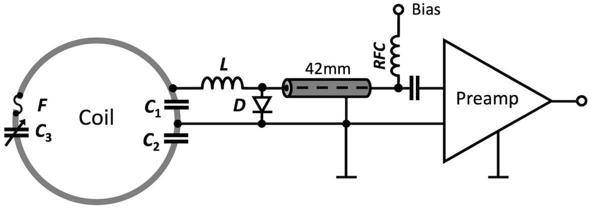
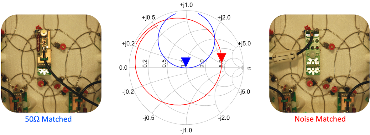
The diameters of the loop coils corresponding to the pentagon/hexagon tiles on the helmet are determined from the size of the pentagon/hexagon tiles; the loop diameter is slightly larger than the diameter of the circle which inscribes the vertexes of the hexagon/pentagons. Next, we construct a pair of test loops to determine the values of the needed capacitors and fine-tune the final size for each coil element. We recommend that the researcher complete these test loops and validate them with imaging tests prior to completing the construction of the larger array. We used 16-awg thick tin-plated copper wire to form the loops with bridges to allow the coil conductors to cross-over one another without touching. We divided each loop symmetrically by two gaps where we place the capacitors (schematic circuit in Figure 2). Thus, each half of the loop is joined at the top by the tuning capacitor and at the bottom by the output-circuit. These two sub-circuits are constructed on separate small circuit boards. The tuning capacitor circuit board contains a variable capacitor C3 to fine-tune the loop resonance to 123.25 MHz (3 Tesla) and a series fuse F for passive protection against large currents potentially induced during transmit. Figure 3 shows the tuning of a single loop with a double probe S21 measure as well as the determination of the quality factor (Q) of the coil both alone and with the other elements in place (Section 4). The output circuit-board (shown in detail in the photo of Figure 4) contains a capacitive voltage divider (C1, C2) to match the elements output to the impedance, ZNM, desired by the preamplifier [8] (Siemens Healthcare, Erlangen Germany) for an optimized noise match. The drive-point circuit board also incorporates an active detuning circuit across the match capacitor. The active detuning is achieved using a PIN diode D in series with a variable inductor L, which together with the match capacitor C1 resonates at the Larmor frequency. Thus, when the PIN diode D is forward biased (transmit mode), the resonant parallel LC1 circuit inserts a high impedance in series with the coil loop, blocking current flow at the Larmor frequency during transmit.4) Coil Quality Factor
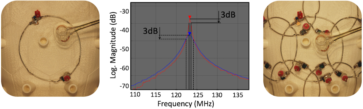
After the determination of the loop sizes and needed components, we calculated the coil Q factor, which describes how much the reactive impedance dominates over the resistive impedance in the loop coil. It informs us of the power dissipated in loss mechanisms relative to the energy stored in the tuned circuit. Under sample-loaded conditions, the resistive impedance is the sum of the coil and sample resistances. We measured the ratio of the coil quality factor in terms of an unloaded (Qunloaded) and a loaded coil (Qload) where the load is the 3D printed head shaped phantom filled with physiological saline and Gadolinium. We measure the ratio of Qunloaded and Qload for both a single loop element and a loop under test surrounded by its six non-resonant neighboring elements. The latter case informs us about the losses in the copper in nearest neighboring elements [2,9]. The procedure for measuring the Q of the loops using a loosely coupled double probe is shown in Figure 5. Care is taken that the probes are not too close to the loop under test (and thus perturbing the measurement) and that conductive material (such as tools and solder) is removed from the area during the test.5) Tuning the Active Decoupling
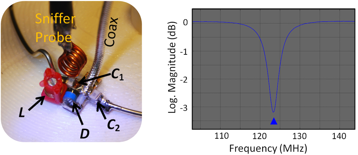
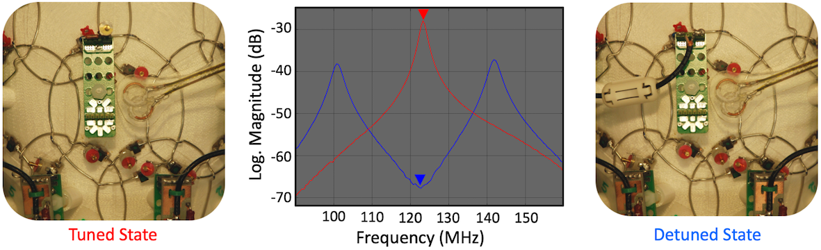
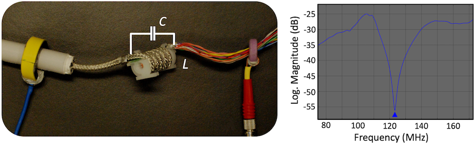
As described above, the trap LC1 together with the pin diode, detune the loop during transmit with the body RF coil. To test that the detuning is adequate, we measure first the tuning of the LC1 circuit using a single pickup loop (“sniffer probe” marked in Figure 4 and Figure 12c) connected to a network analyzer S11. This trap circuit tuning step is done without the main coil loop being tuned (variable capacitor was still missing) and with the PIN diode forward biased (conductive state). After initial tuning of the trap circuit with the small sniffer probe, we attached the variable capacitor C3 to close the circuit of the main loop and tuned the coil to 123.25 MHz using a double probe controlled via the S21 measurement. Holding the double probe on the same position, but actively switching the forward bias of the PIN diode on an off, we measure the loop response in the tuned and detuned state (Figure 4 middle). We expect the active detuning to produce S21 > 35 dB isolation between these two states (Figure 4).6) Preamplifier Decoupling
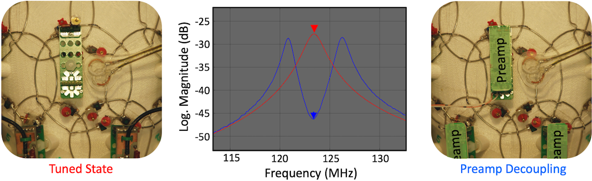
Preamplifier decoupling is used to reduce coupling between next-nearest and further neighbors. It has become one of the most important tools in constructing Rx arrays [10]. Optimization of the preamplifier decoupling is a critical step in constructing highly parallel arrays. The goal is to design the preamplifier/coil circuit so that the preamplifier performs a voltage measurement across the loop. Thus the output circuitry (match + coax + preamplifier) forms a series high impedance in the tuned loop reducing current flow and thus reducing inductive coupling with other loop elements.To transform the preamplifier input impedance to a high impedance in the loop, we first transformed it to a low impedance (short-circuit) across a parallel LC circuit (L and C1 in Figure 2) tuned to the Larmor frequency. This parallel LC circuit, in turn, introduces a high serial impedance in the coil loop. In this mode, minimal current flows in the loop and inductive coupling to other coils is minimized. We used the same L and C1 for the active detuning trap. We closed the parallel LC1 circuit by transforming the preamplifier input impedance to a short across the PIN diode shown in Figure 3. This is done by carefully controlling the cable length (42 mm in this case) between preamplifier and coil terminal so that it transforms the input impedance of the preamplifier to a short across the diode.
We adjust the preamplifier decoupling viewing the S21 versus frequency for the coil in the tuned state (PIN diode reverse biased) with the preamp in place and powered on using the same decoupled double probe, but with reduced power output from the network analyzer (-25 dBm). It is important that the minimum of the S21 “dip” is at the Larmor frequency (Figure 6) thus verifying that the correct impedance transformation at the Larmor frequency was performed. Low-loss circuitry between the preamp input and the loop insures a high degree of preamplifier decoupling which can be indirectly measured by assessing the depth of the "dip" in Figure 6.
If a quantitative measure of the preamplifier decoupling is desired, the measurement can be repeated with the preamplifier replaced by a load with the conjugate complex impedance Z*NM of the preamplifier’s noise-match impedance ZNM. We constructed of a dummy preamplifier board with a conjugate complex input impedance Z*NM. Then a comparison of the S21 at the Larmor frequency with this board and with the preamp quantifies the preamplifier decoupling [11].
7) Determining the Critical Overlap
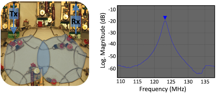
In this step the overlap between neighboring elements is adjusted to null their mutual inductance [12]. Before performing this step, we must have completed the loop and active decoupling tuning of Section 4 for all loops on the helmet. We estimated the critical overlap ratio of a pair of loops by carefully moving those loops towards each other while measuring the S21 parameter between the tuned coils (with any other loops biased to the detuned state using their active decoupling circuit). We monitor the S21 interaction between the two neighbouring coils using a test probe that plugs into the circuit board at the position of the preamplifier (Figure 7). In our case, the impedance of the circuit at this point is not 50 Ω. Thus, we needed to temporarily transform this load impedance to the 50 Ω input impedance of the network analyzer for this measurement. This transformation (from ZNM to the 50 Ω expected by the network analyzer) is done on the test probe we plug into the preamplifier socket (Figure 7). If a preamplifier with 50 Ω noise match requirements is used, this step can be omitted.The critical overlap ratio between the loop diameter and the center-to-center distance from two adjacent loops was found to be 0.76 and provides a decoupling of < -17 dB (Figure 7). We compare this center-to-center spacing to that assumed in the hexagonal/pentagonal tiling and fine-tune the loop diameters as needed.
8) Array Assembly
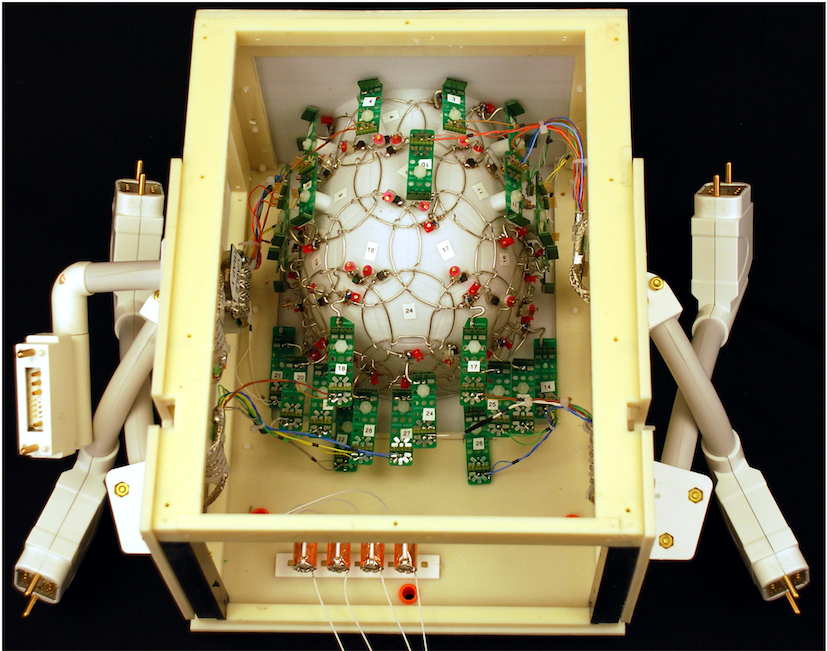
After successfully testing the first loops, we assembled the whole array: First, all the drive points and capacitor solder pads, made out of FR4 circuit material, were mounted on the helmet. Second the 16-awg thick tin-plated copper wires are cut, bent and assembled over the whole array. Third, the preamplifier board including the 42 mm long coaxial cable were mounted to the designated holder (Figure 8), as well as wiring up the preamplifier and bias tee circuitry to the plug cables. All preamps were carefully orientated along the z-direction to minimize Hall effect issues [13-15]. Fourth, the detuning traps on the drive were adjusted to be resonant at the Larmor frequency when the PIN diode was forward biased, as described in Section 4.9) Geometrical Nearest-Neighbor Decoupling of the Array
The goal of the geometrical decoupling is to find a critical overlap of all adjacent coils in order to minimize the mutual decoupling between any pair of neighboring coils. To achieve this, we monitor the S21 interaction between two neighboring coils using the probe that plugs into the circuit board at the position of the preamplifier (Figure 8) as described in Section 6. This optimization of all next neighbors is the most time consuming adjustment procedure during phased array construction.With a pair of coils hooked up to the network analyzer using the impedance transforming sockets, we measure S21 between each adjacent pair with all other coils detuned using their active detuning circuits. We minimized S21 by empirically bending the crossing bridges on the loops. After each bending, the impedance of the loop is often altered, and we need to readjust the test probe to keep the 50 Ω impedance expected by the network analyzer. We also re-adjust the tuning of the loop (variable capacitor C3). The achieved geometrical decoupling in the array ranged from -16 dB and -21 dB. After completing all combinations of elements, we repeated all these adjustments with a second go-thru.
10) Tuning and Matching
After the geometrical decoupling, each element needs to be retuned and matched to the preamplifier’s noise matched condition. This is done using a direct S11 measurement with cables directly connected to the preamplifier sockets of the element under test (Figure 9 right photo). It is important that the electrical delay produced by the probe is accurately calibrated. When adjusting the tuning and matching all other unused elements of the phased-array are detuned. This procedure is done with the array loaded with a tightly fitted head-shaped phantom.11) Final Bench Touch Up
The final step of phased-array construction is a careful check up of the loop tuning, active detuning, and preamplifier decoupling. This step was done with all of the preamplifiers present and the array plugged into a simulator that passes the PIN diode biases and DC power to each preamp from the scanner. Starting with all of the array elements in the detuned states (i.e. all PIN diode bias set to forward bias the diode in each element), the bias voltage for a given loop was toggled on and off while the detuning is monitored using a double inductive probe and the S21 measurement (again Figure 4). A fine adjusting of the detuning inductor is sometimes needed to achieve this. After this step, we verify the preamplifier decoupling by viewing the S21 versus frequency for the coil in the tuned state using the same decoupled double probe, but with reduced power output from the network analyzer (-25 dBm). It is important that the minimum of the S21 “dip” is at the Larmor frequency (Figure 6). Note that this measurement requires that the preamplifier is powered on. Finally the cable traps on each plug were checked and adjusted via an S21 measurement using current probes (Figure 10). The final array coil is shown in Figure 11.12) Customized Bench Tools
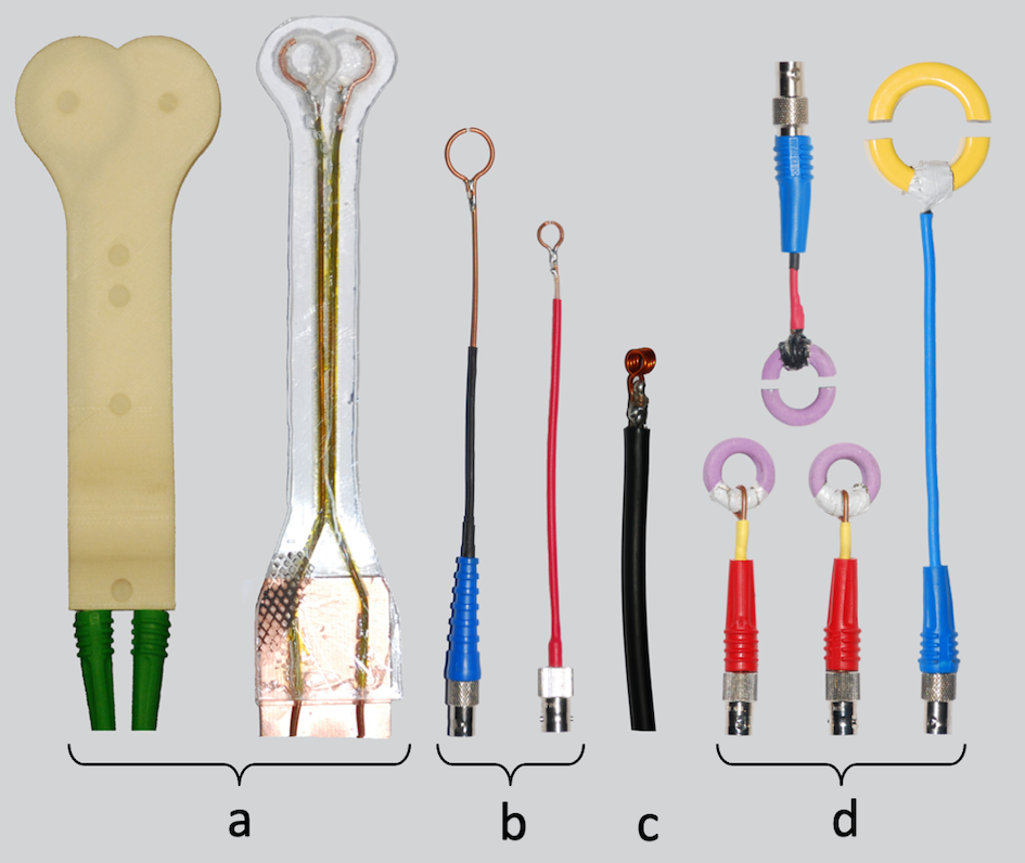
Handcrafted RF probes are commonly used in MRI coil construction. The most popular probe at the bench is the "double probe" (Figure 12a), which is used at almost every stage of array coil construction. The probe consists of two overlapped loops made out of semi-rigid coax cable with a gap in the shield placed symmetrically in the middle of each loop. The decoupling of both loops should be >70 dB. Single magnetic field probes in different sizes are also useful for various applications (Figure 12b). The small "sniffer" probe is useful to sniff out sources of resonances in circuits (e.g. isolated detuning traps). It consists of a small solenoid coil attached to the end of a coax cable (Figure 12c). Current probes are used for adjustments of common mode current traps. They are made out of a ferrite core and a single turn semi-rigid coax cable (including shield gap) (Figure 12d). For good accessibility in various measurement situations, it is helpful to have the possibility for opening up the current probe.Acknowledgements
Thanks to Alina Scholz, Nicolas Kutscha, Matthäus Poniatowski, Markus W May, Robin Etzel, Mirsad Mahmutovic, Anpreet Ghotra, Chaimaa Chemlali, Gurinder Kaur Multani, Hans K Hartmann, Manisha Shrestha, and Sam-Luca JD Hansen.References
[1] B. Keil, L. L. Wald, Massively Parallel MRI Detector Arrays, J. Magn. Reson. (2013) 229:75-89.
[2] G. C. Wiggins, J. R. Polimeni, A. Potthast, M. Schmitt, V. Alagappan, L. L. Wald, 96-Channel receive-only head coil for 3 Tesla: design optimization and evaluation, Magn. Reson. Med. 62 (2009) 754–762.
[3] B. Keil, J. N. Blau, S. Biber, P. Hoecht, V. Tountcheva, K. Setsompop, C. Triantafyllou, L. L. Wald, A 64-channel 3T array coil for accelerated brain MRI, Magn. Reson. Med. (2013) 70:248-58.
[4] M. Schmitt, A. Potthast, D. E. Sosnovik, J. R. Polimeni, G. C. Wiggins, C. Triantafyllou, L. L. Wald, A 128-channel receive-only cardiac coil for highly accelerated cardiac MRI at 3 Tesla, Magn. Reson. Med. 59 (2008) 1431–1439.
[5] C. J. Hardy, R. O. Giaquinto, J. E. Piel, K. W. Rohling, L. Marinelli, D. J. Blezek, E. W. Fiveland, R. D. Darrow, T. K. F. Foo, 128-channel body MRI with a flexible high-density receiver-coil array, J. Magn. Reson. Imaging 28 (2008) 1219–1225.
[6] B. Keil, V. Alagappan, A. Mareyam, J. A. McNab, K. Fujimoto, V. Tountcheva, C. Triantafyllou, D. D. Dilks, N. Kanwisher, W. Lin, P. E. Grant, L. L. Wald, Size-optimized 32-channel brain arrays for 3 T pediatric imaging, Magn. Reson. Med. 66 (2011) 1777–1787.
[7] G. C. Wiggins, C. Triantafyllou, A. Potthast, A. Reykowski, M. Nittka, L. L. Wald, 32-channel 3 Tesla receive-only phased-array head coil with soccer-ball element geometry, Magn. Reson. Med. 56 (2006) 216–223.
[8] M. Hergt, R. Oppelt, M. D. Vester, A. Reykowski, K. M. Huber, K. Jahns, H. J. Fischer, Low noise preamplifier with integrated cable trap, Proceedings of the 15th Annual Meeting of ISMRM, Berlin, (2007) p. 1037.
[9] A. Kumar, W. A. Edelstein, P. A. Bottomley, Noise figure limits for circular loop MR coils, Magn. Reson. Med. 61 (2009) 1201–1209.
[10] P. B. Roemer, W. A. Edelstein, C. E. Hayes, S. P. Souza, O. M. Mueller, The NMR phased array, Magn. Reson. Med. 16 (1990) 192–225.[
11] A. Reykowski, S. M. Wright, J. R. Porter, Design of matching networks for low noise preamplifiers, Magn. Reson. Med. 33 (1995) 848–852.
[12] J. S. Hyde, A. Jesmanowicz, W. Froncisz, J. B. Kneeland, T. M. Grist, N. F. Campagna, Parallel image acquisition from noninteracting local coils, J. Magn. Reson. 70 (1986) 512–517.
[13] C. Possanzini, M. Bouteljie, Influence of magnetic field on preamplifiers using GaAs FET technology, Proceedings of the 16th Annual Meeting of ISMRM, Toronto, (2008) p. 1123.
[14] D. I. Hoult, G. Kolansky, A Magnetic-Field-Tolerant Low-Noise SiGe Pre-amplifier and T/R Switch, Proceedings of the 18th Annual Meeting of ISMRM, Stockholm, (2010) p. 649.
[15] R. Lagore, B. Roberts, B. G. Fallone, N. De Zanche, Comparison of Three Preamplifier Technologies: Variation of Input Impedance and Noise Figure With B0 Field Strength, Proceedings of the 19th Annual Meeting of ISMRM, Montreal, (2011) p. 1864.
Figures