1407
Gallium nitride MOSFETs enable transmit-receive switching in less than 100ns1Institute for Biomedical Engineering, ETH Zurich and University of Zurich, Zürich, Switzerland
Synopsis
For short-T2 MRI measurements, fast T/R switches that can handle high RF power are of paramount importance. In this work, we present a T/R switch based on GaN MOSFETs that switches in tens of nanoseconds and can handle a peak power of more than 1000W.
Introduction
For imaging compounds with very short coherence life times, minimizing the time between spin excitation and the start of the signal acquisition is of crucial importance [1].One important contribution to this dead time is the time it takes for the transmit-receive (T/R) switch to change state. Except at low field [2], switch designs are nowadays based on PIN diodes, which are comparably slow when high RF power is required. The fastest existing T/R switch for MRI has an overall switch time below 1µs with a rise time of 350ns [3]. As an alternative to PIN diodes, GaN MOSFETs are known to be able to switch rapidly and have been used for active detuning and Q-spoiling [4,5,6].
In this work, we present the first T/R switch based on gallium nitride (GaN) MOSFETs with a switching time below 100ns at high power levels.
Methods
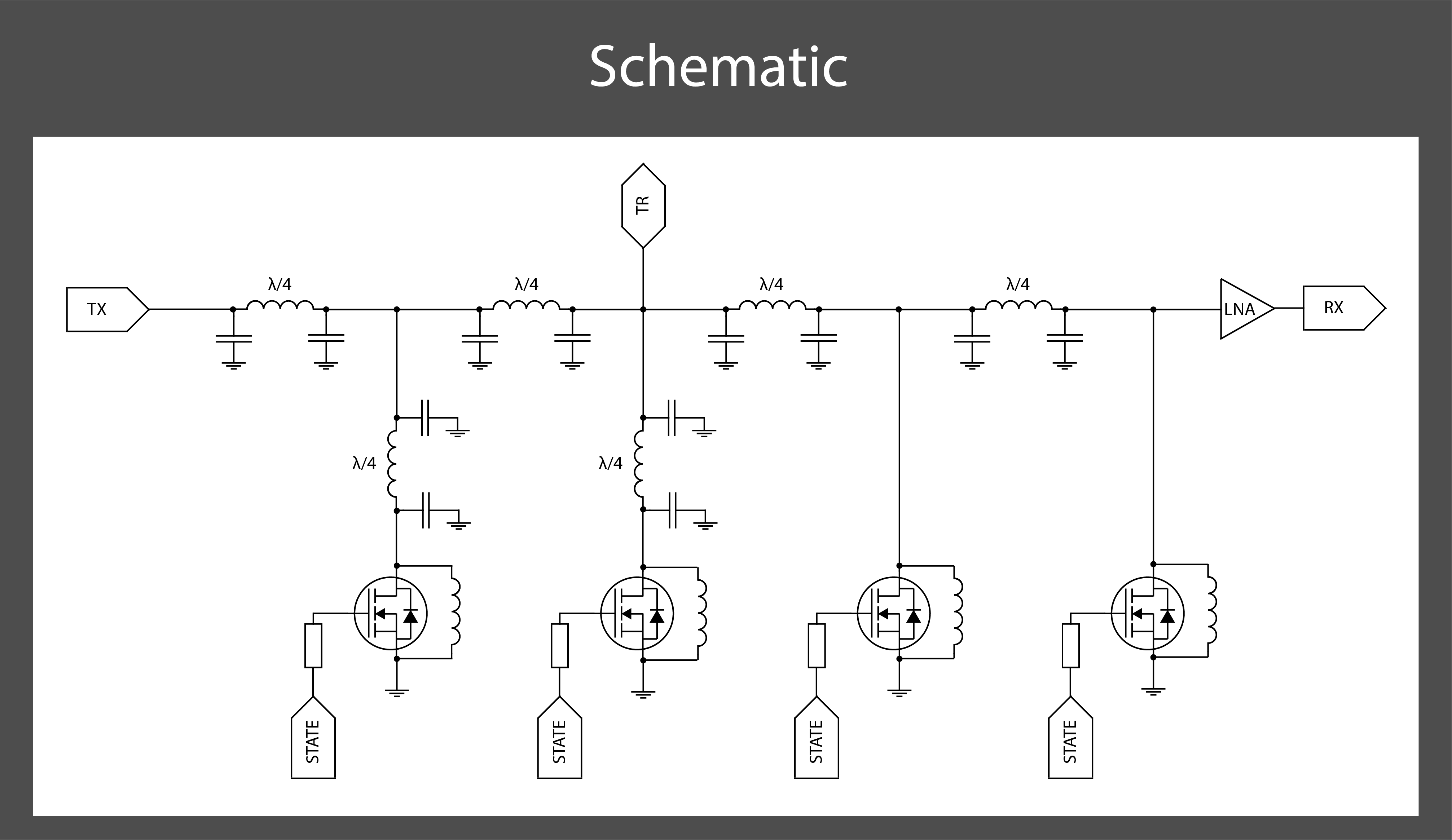
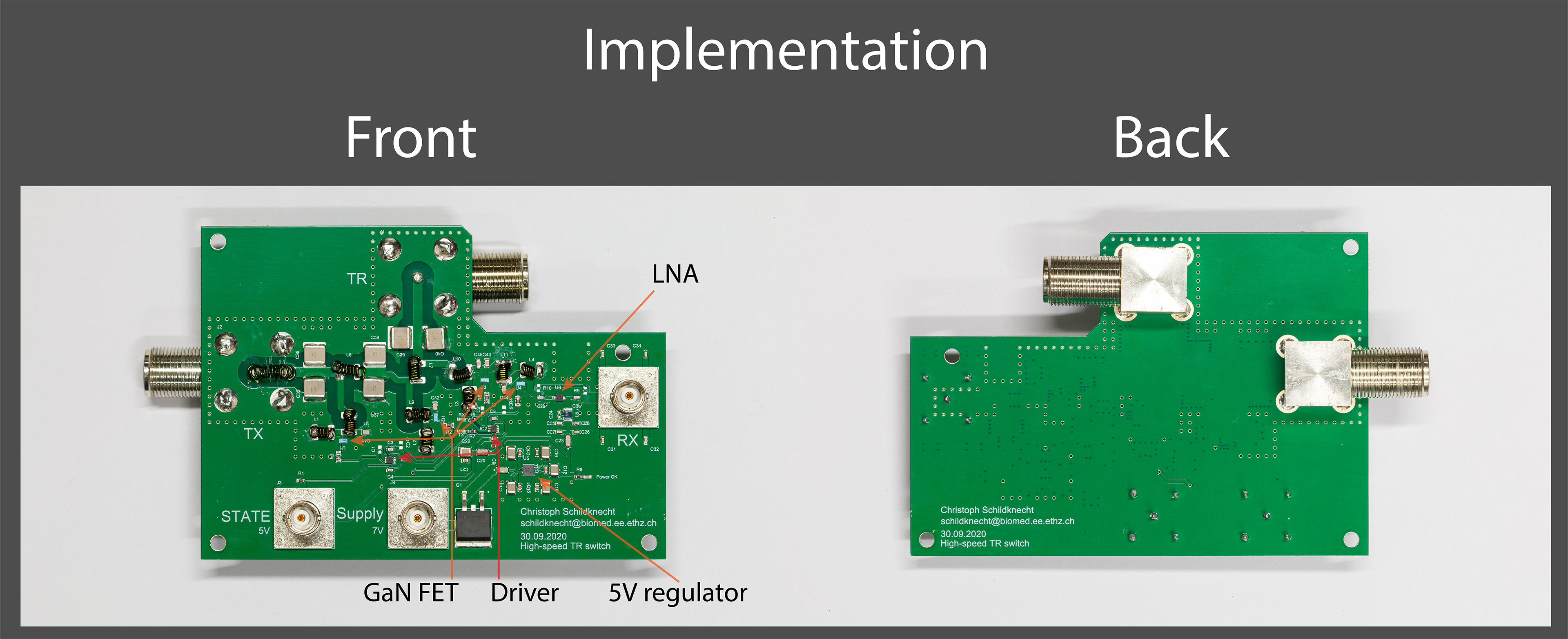
The topology utilized for the proposed T/R switch is shown in Fig. 1. The key for this T/R switch is the utilization of GaN MOSFETs which have an output capacitance of a few tens of picofarads. As such, they can present a high impedance at the Larmor frequency in the off-state when a matching inductor is connected in parallel to the drain source terminals. Such a GaN MOSFET can be implanted into a quarter-wave arrangement as shown in Fig. 1, which implements a single pole double throw (SPDT) network. In the transmission state, all the MOSFETs are in the on-state were they conduct RF currents well isolating the RX port from the high-power RF. In the reception state, all the MOSFETs are in their off-state passing the RF power from the TR port to the RX port and isolating the TX port.An implementation of such a topology for a 3T system with a Larmor frequency of 128MHz is shown in Fig. 2. The two-layer PCB has an additional low noise amplifier (LNA) on board.
The coupling parameters of this implementation were measured with an Agilent Technologies E5071C network analyzer. To measure the transient response, an Agilent Technologies MSO7054A oscilloscope, an R&S SMB 100A signal generator, an Agilent Technologies 81104A pulse-pattern generator, a National Instruments PXIe-5622 16-bit digitizer and a Bruker BLA-1000 amplifier were used. Thermal images were taken with a Fluke TiS20.
For MR measurements Zero-echo-time (ZTE) imaging with algebraic reconstruction [8] was performed with a setup based on a Philips Achieva 3T scanner, equipped with a high-performance insert gradient [7] and complemented with a Bruker BLA-1000 amplifier and an R&S SMB 100A.
Results
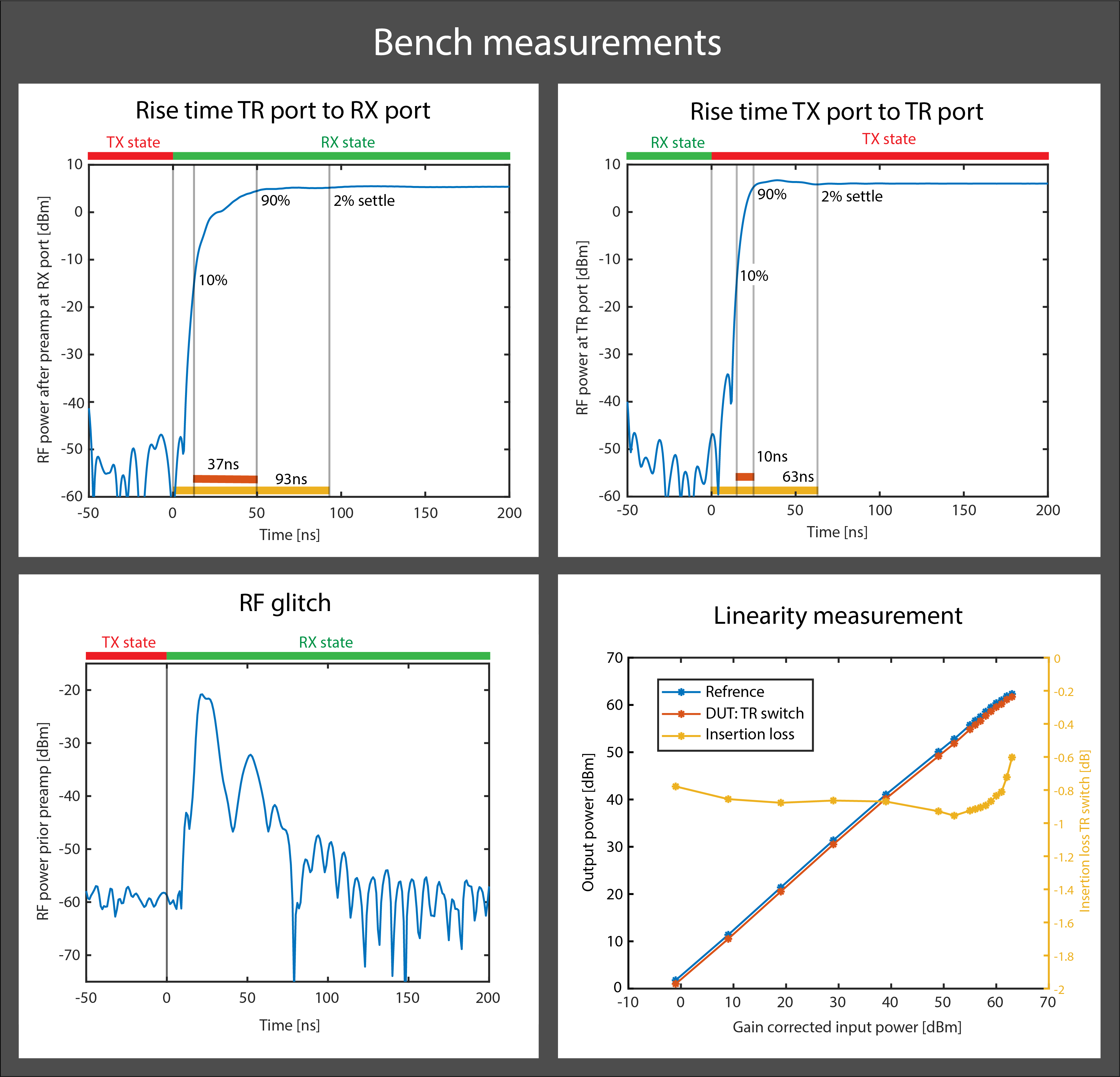
At the operation frequency of 128MHz, the insertion loss from the TX to the TR port in the transmit state is -0.35dB and the insulation to the RX port is -66.3dB. In the receive state the insertion loss from the TR port to the RX port is -0.8dB and the insulation towards the TX port is -74.3dB.Bench measurements are shown in Fig. 3. Based on these findings, the switching time was assessed at less than 100ns with a rise time of 35ns. The signal glitch introduced by the switching event peaked at -20dBm with a decay of 10dB every approximately 30ns. The assessment of the linearity shows little alteration in insertion loss up to 60dBm. Above 60dBm up to approximately 62dBm the insertion loss slightly decreased which might be attributed to impedance-dependent power amplifier gain above the nominal output power.
Evaluation of the power consumption with 7V input voltage, excluding the LNA, resulted in a power consumption of 30.8mW idle and 35.7mW with a TR of 25µs and TX pulse length of 1µs. Almost all (30.1mW) of the static power is drawn by the ADM7150 ultralow noise RF LDO which feeds also the LNA.
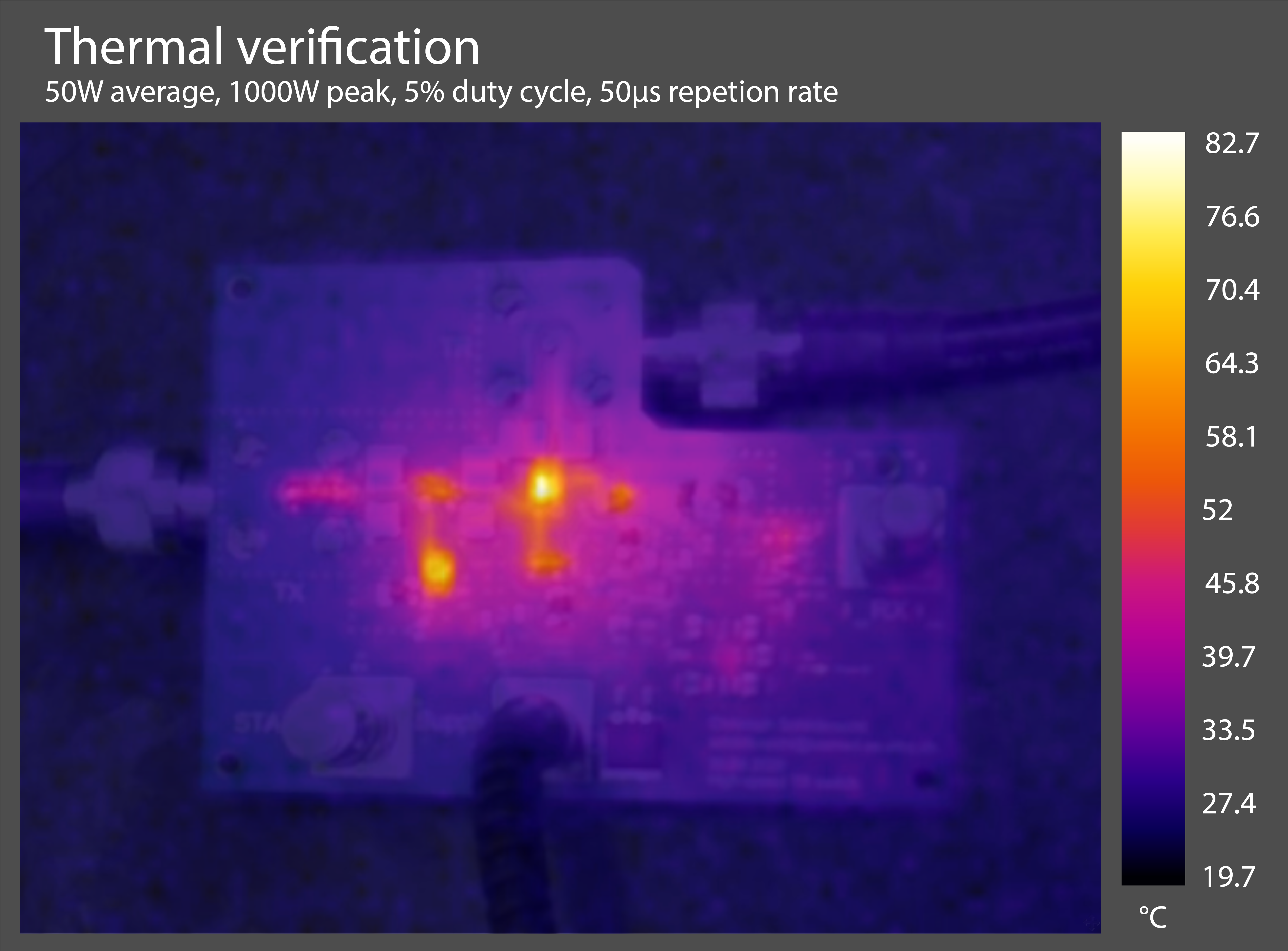
The thermal image in Fig. 4 shows that the temperatures of the T/R switching are well under control when applying 50W average and 1000W peak input power. The hottest component is an inductor with a temperature of 82.7°C. The GaN MOSFETs do not appear to be particular hotspots.
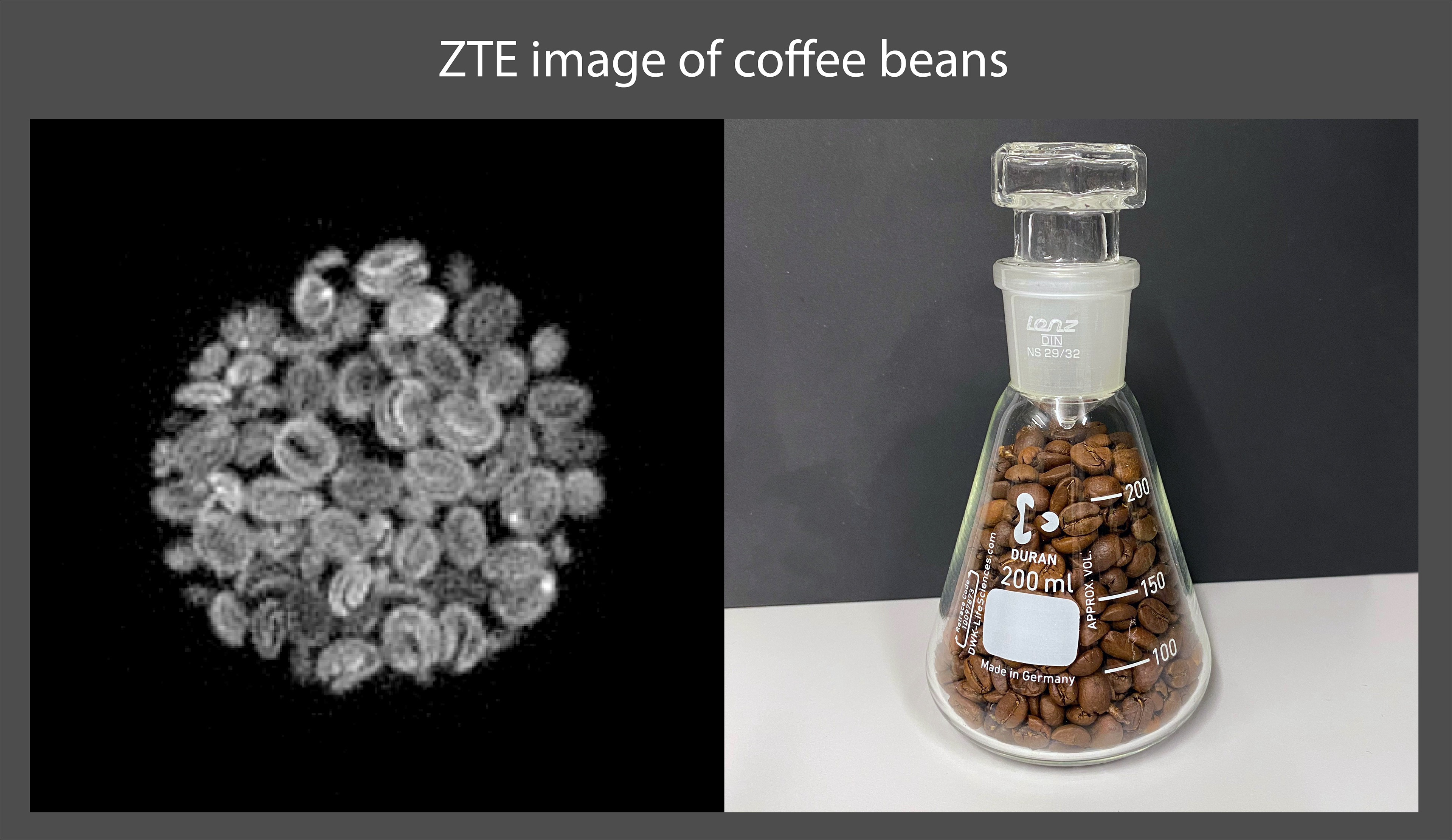
ZTE imaging of the coffee bean phantom is shown in Fig. 5 and does not indicate any artifacts related to T/R switching.
Discussion and conclusion
The presented GaN T/R switch enables switching from transmit to receive state in less than 100ns. This is especially of interest when observing compounds with very short coherence times, as for example the myelin bilayer in the brain, which has signal components with T2s down to 8us [9].For taking full advantage of such a T/R switch, the rest of the RF signal chain needs to be highly capable as well. Besides RF power amplifier fall time, most certainly coil ring-down suppression of the MRI coil is required because this may take hundreds of nanoseconds up to a microsecond. However, there are already several proposals on how to tackle coil ring-down [10,11,12].
In addition to RF performance, the proposed T/R switch utilizes besides the connectors only SMD components. Those components are placed only on one side, which simplifies the assembly. Further, for driving the MOSFETs only a unipolar supply is needed and can be done by a logic IC, thus making the design easy to integrate and operate.
Acknowledgements
No acknowledgement found.References
[1] Weiger, M., Pruessmann, K.P. and Hennel, F. (2011), MRI with zero echo time: Hard versus sweep pulse excitation. Magn. Reson. Med., 66: 379-389. https://doi.org/10.1002/mrm.22799
[2] P.-J. Nacher, S. Kumaragamage, G. Tastevin and C. P. Bidinosti, "A fast MOSFET RF switch for low-field NMR and MRI", J. Magn. Reson., vol. 310, Jan. 2020.
[3] Brunner, D.O., Furrer, L., Weiger, M., Baumberger, W., Schmid, T., Reber, J., Dietrich, B.E., Wilm, B.J., Froidevaux, R., Pruessmann, K.P., 2016. Symmetrically biased T/R switches for NMR and MRI with microsecond dead time. J. Magn. Reson. https://doi.org/10.1016/j.jmr.2015.12.016
[4] J. Y. Lu et al., "Depletion-Mode GaN HEMT Q-Spoil Switches for MRI Coils," in IEEE Transactions on Medical Imaging, vol. 35, no. 12, pp. 2558-2567, Dec. 2016, doi: 10.1109/TMI.2016.2586053.
[5] M. Twieg, M. A. de Rooij and M. A. Griswold, "Active Detuning of MRI Receive Coils with GaN FETs," in IEEE Transactions on Microwave Theory and Techniques, vol. 63, no. 12, pp. 4169-4177, Dec. 2015, doi: 10.1109/TMTT.2015.2495366.
[6] M. Twieg, M. D. Rooij, and M. A. Griswold, “Enhancement mode GaN on silicon (eGaN FETs) for coil detuning,” Proc. Int. Soc. Magn. Reson. Med., vol. 22, p. 926, 2014.
[7] Weiger, M., Overweg, J., Rösler, M.B., Froidevaux, R., Hennel, F., Wilm, B.J., Penn, A., Sturzenegger, U., Schuth, W., Mathlener, M., Borgo, M., Börnert, P., Leussler, C., Luechinger, R., Dietrich, B.E., Reber, J., Brunner, D.O., Schmid, T., Vionnet, L. and Pruessmann, K.P. (2018), A high‐performance gradient insert for rapid and short‐T2 imaging at full duty cycle. Magn. Reson. Med, 79: 3256-3266. https://doi.org/10.1002/mrm.26954
[8] Weiger M, Pruessmann KP. MRI with zero echo time. eMagRes. Volume 1. Chichester, United Kingdom: John Wiley & Sons, Ltd; 2012. p 311-322.
[9] Markus Weiger, Romain Froidevaux, Emily Louise Baadsvik, David Otto Brunner, Manuela Barbara Rösler, Klaas Paul Pruessmann, Advances in MRI of the myelin bilayer, NeuroImage, Volume 217, 2020, https://doi.org/10.1016/j.neuroimage.2020.116888.
[10] Troy W. Borneman, David G. Cory (2012), Bandwidth-limited control and ringdown suppression in high-Q resonators, JMR, https://doi.org/10.1016/j.jmr.2012.10.011
[11] A.S. Peshkovsky, J. Forguez, L. Cerioni, D.J. Pusiol, 2005, RF probe recovery time reduction with a novel active ringing suppression circuit, JMR, https://doi.org/10.1016/j.jmr.2005.07.004.
[12] D. O. Brunner, K. P. Pruessmann, (2014), Coil Ringdown Suppression by Broadband Forward Compensation, Proc. Intl. Soc. Mag. Reson. Med. 22
Figures