4243
Radiated Noise Reduction for a Gradient Driver with SiC MOSFETs using Double Shielding
Juan Sabate1, Huan Hu1, Ruxi Wang2, and Logan Snow1
1GE Global Research, Niskayuna, NY, United States, 2GE Aviation, Dayton, OH, United States
1GE Global Research, Niskayuna, NY, United States, 2GE Aviation, Dayton, OH, United States
Synopsis
The gradient driver was implemented with SiC MOSFETs. The
amplifier has less losses and is more compact, however switching has higher
high frequency contents. The new amplifier was tested in an EMI shielded room.
The results show the effectiveness of the double shielding method at reducing
the radiated noise generated by a gradient driver system. The tests confirmed
the correlation between the conducted and radiated noise. The double shielding
method proposed reduced the radiated noise caused by the CM circulating current
between cables. The measurements showed up to 35dB radiated noise reduction
with this method.
Introduction
In an MRI system, the gradient driver is a switching power converter implemented with power semiconductor devices, such as insulated gate bipolar transistors (IGBTs), power metal oxide semiconductor field effect transistors (MOSFET), etc. [1]. To control the electrical power that can be transferred by the gradient driver, the power semiconductor devices are usually controlled with pulse width modulation (PWM) with high voltage, high current and high switching frequency. New advanced power semiconductor devices, like silicon carbide (SiC) MOSFETs, could have less losses and sustain higher voltage which will simplify the power supply architecture and make the gradient amplifier more efficient than the silicon version. However, the SiC fast switching will lead to a faster voltage (dv/dt) or current (di/dt) transient which could generate greater high frequency harmonic content [1-6]. The fast rise and fall times of the SiC device switching has higher high frequency contents shown in Fig 1. The high frequency harmonic contents may contaminate radio frequency (RF) signals that will be sensed by RF coils, and lead to a significant degradation of MR image quality. Therefore, it is desired to decrease the electromagnetic noise generated by the gradient driver.Silicon Carbide (SiC) Gradient Driver
The new wideband gap devices made of materials such as SiC provide a much higher bandgap, breakdown field, and thermal conductivity which offer them the potential capability to overcome the frequency, temperature and power management limitations of traditional silicon devices. Fig.2a shows the improved two H-bridge cascaded structure with high voltage (1700V) SiC MOSFETs. The modular structure brings the benefit of lower component volume, simpler implementation and lower loss. Fig. 2b shows one of the H-bridges for the gradient driver prototype presented in [6].Baseline Noise Measurement without the Double Shielding Method
The gradient driver is placed in an EMI shielded room for noise level measurement. Beside the DC input cables, two other cables, the gate driver power supply and current sensor cables, are connected from outside the EMI room through a penetration panel. All the cables are shielded. This setup sketch is shown Fig. 4a. The radiated noise measured by a bi-conical antenna and it is shown in Fig.5a. At the frequency range of interest, the broadband noise is around -170dBm and the noise spikes are around -132dBm. In order to pinpoint the noise source and correlate it with the conducted noise, common mode (CM) conducted noise from each cable is also measured, as shown in Fig.3. On the conducted noise measurement results, very similar CM current patterns can be observed. This similar pattern indicate that CM circulating current exists between cables. Therefore, a better shielding method is desired to reduce the radiated noise generated from the CM circulating current.Double Shielding Method & Results
In order to reduce the circulating CM current between cables, the double shielding method is proposed. The schematic of the double shielding method is shown in Fig.4b. First, all the connecting cables are tied together, and multiple grounding points are removed to reduce the large CM loop. Meanwhile, a shielding pipe is utilized outside the connecting cables to shield the radiated noise caused by the circulating current between the multiple cables. In the experiment setup, an aluminum shielding pipe is utilized. The effectiveness of the shielding method is demonstrated through the radiated noise measurement. As shown from Fig.5b, the noise spikes decrease up to 35dB and the broadband noise decreases around 5dB.Conclusion
The gradient driver implemented with SiC MOSFETs was tested in an EMI shielded room. The results show the effectiveness of the double shielding method at reducing the radiated noise generated by a gradient driver system. The tests confirmed the correlation between the conducted and radiated noise. The double shielding method proposed reduced the radiated noise caused by the CM circulating current between cables. The measurements showed up to 35dB radiated noise reduction with this method.Acknowledgements
No acknowledgement found.References
[1] J. Sabate, et al., Proc. ISMRM. 2007. [2] A. Gupta, IEEE Trans on Power Electronics pp: 1672-1681, 2007. [3] R. Wang, et al., Proc. IEEE ECCE 2014. [4] R. Wang, et al. Proc. IEEE ECCE 2015, [5] F. Wang, et al., IEEE Trans. on Industry Applications. pp. 1336-1341, 2000. [6] R. Wang, et al. Proc. ISMRM 2017.Figures
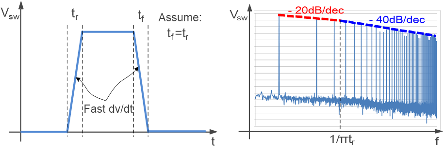
Fig. 1 Frequency content with related rise and fall
times
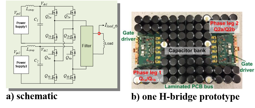
Fig.2 Two bridge gradient driver with SiC module
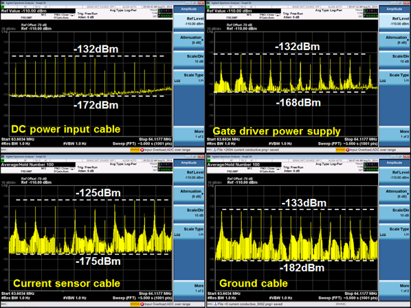
Fig. 3 Conducted noise measurement (Top row, left
to right: DC power input, gate driver power supply, Bottom row; Left to right: current sensor, ground)
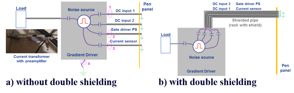
Fig.4 Gradient driver connection in the EMI
shielding room
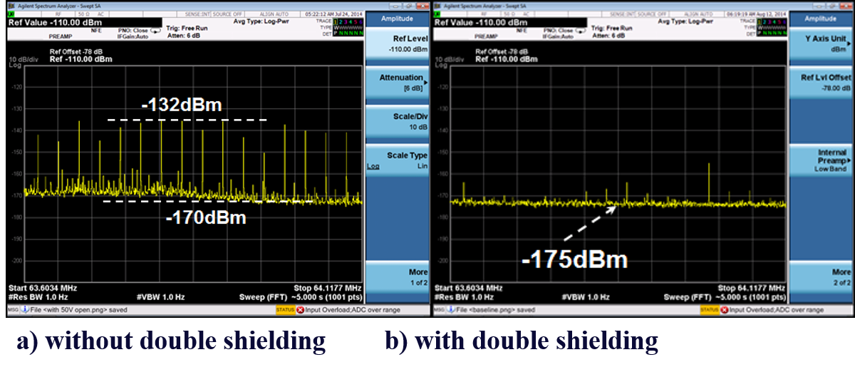
Fig.5 Radiated noise
measurement