1133
In-bore voltage inversion with very low EMI by a switched capacitor converter1ETH Zurich and University of Zurich, Zurich, Switzerland
Synopsis
Complex in-bore electronics (e.g. motion trackers, digitizer etc.) frequently requires various voltage rails. This poses especially a challenge when bi-polar voltages are required because in-bore voltage inversion is typically not possible due to the EMI of such converter. The here presented switched capacitator voltage inverter allows in-bore operation without disturbing the MRI scanner due to the very low EMI. Lab and 3T MRI measurement were performed to verify the EMC compatibility and characterize the device.
Introduction
Increasingly more complex electronics is deployed in the bore of MRI scanners e.g. for motion tracking, RF digitization, PET detection, actuation systems etc. These devices typically require various supply voltage rails. Routing them individually into the bore by separate lines comes with RF compliance, usability and safety issues [1-4]. Alternatively, linear voltage regulators are deployed providing accurate voltages locally, however inflicting substantial power losses and not providing voltages that are higher or of opposite polarity than the primary supply. Switching converters would provide a standard solution to this problem. Unfortunately, their noise emissions and inductance requirements often enforcing the use of extensive shielding and ferrite materials typically prohibits their usage in the bore [1]. In this work, we hence evaluate switched capacitor voltage inverters for powering in-bore electronics in particular with respect to their noise emission properties.Methods
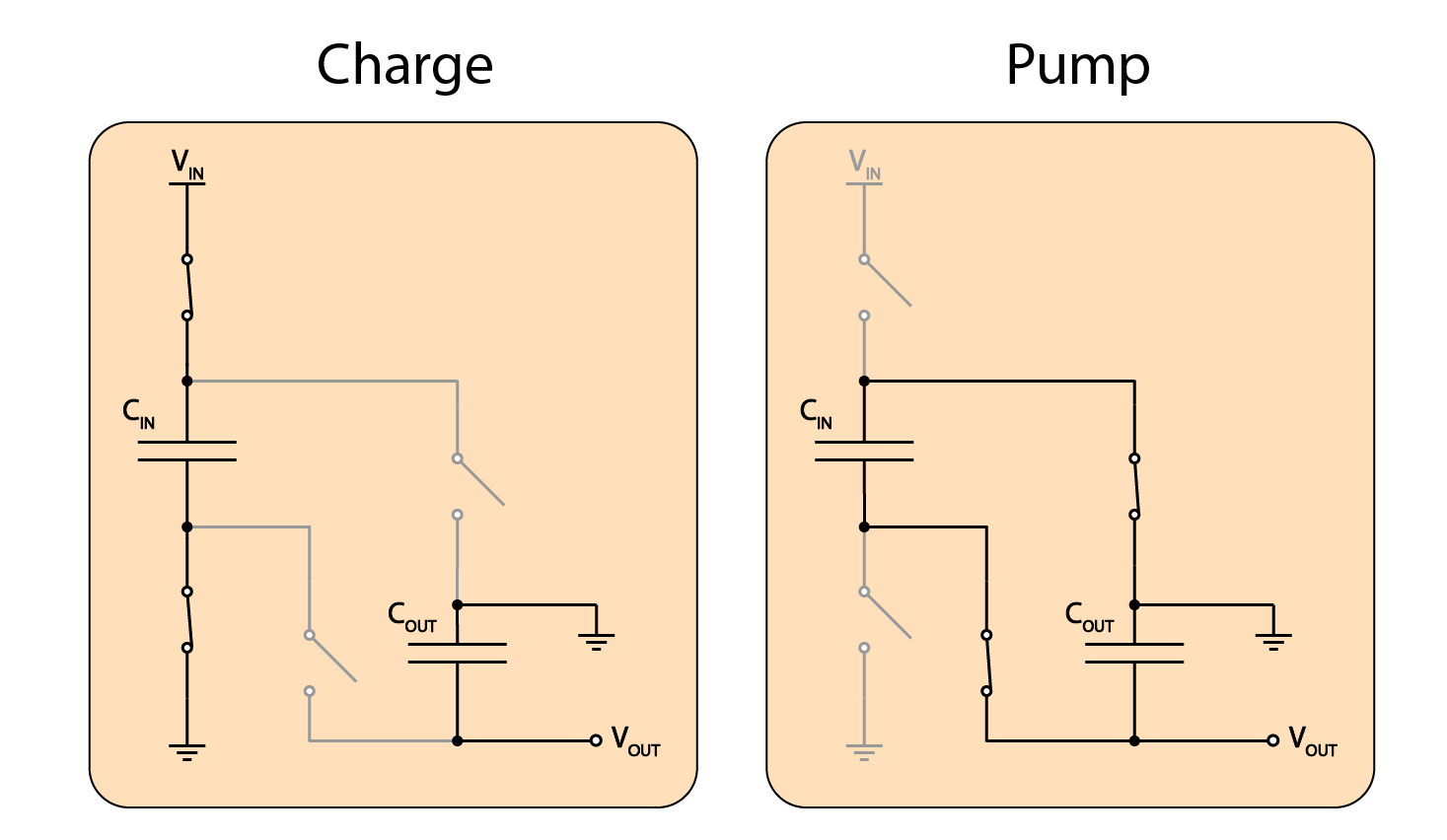
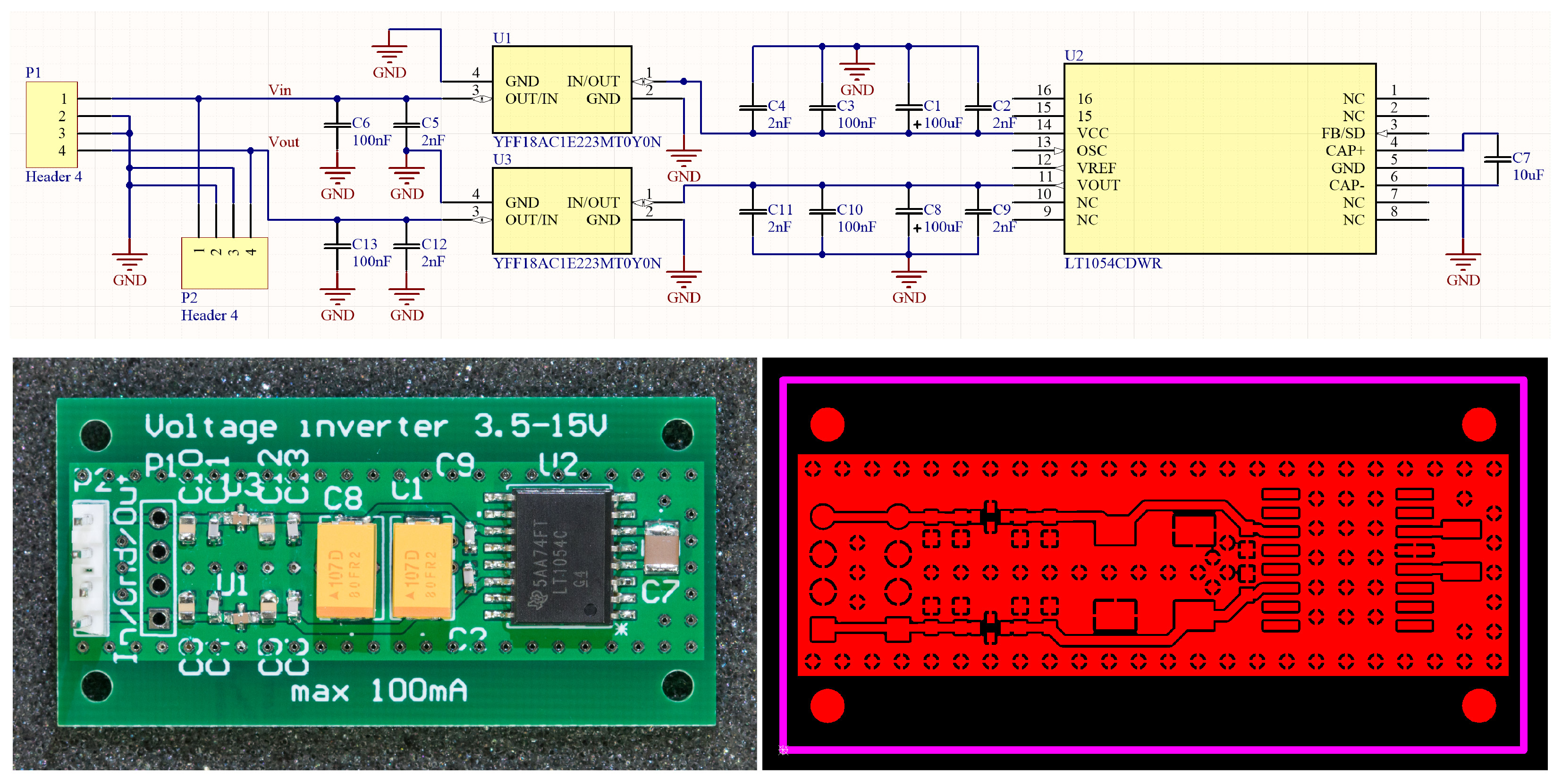
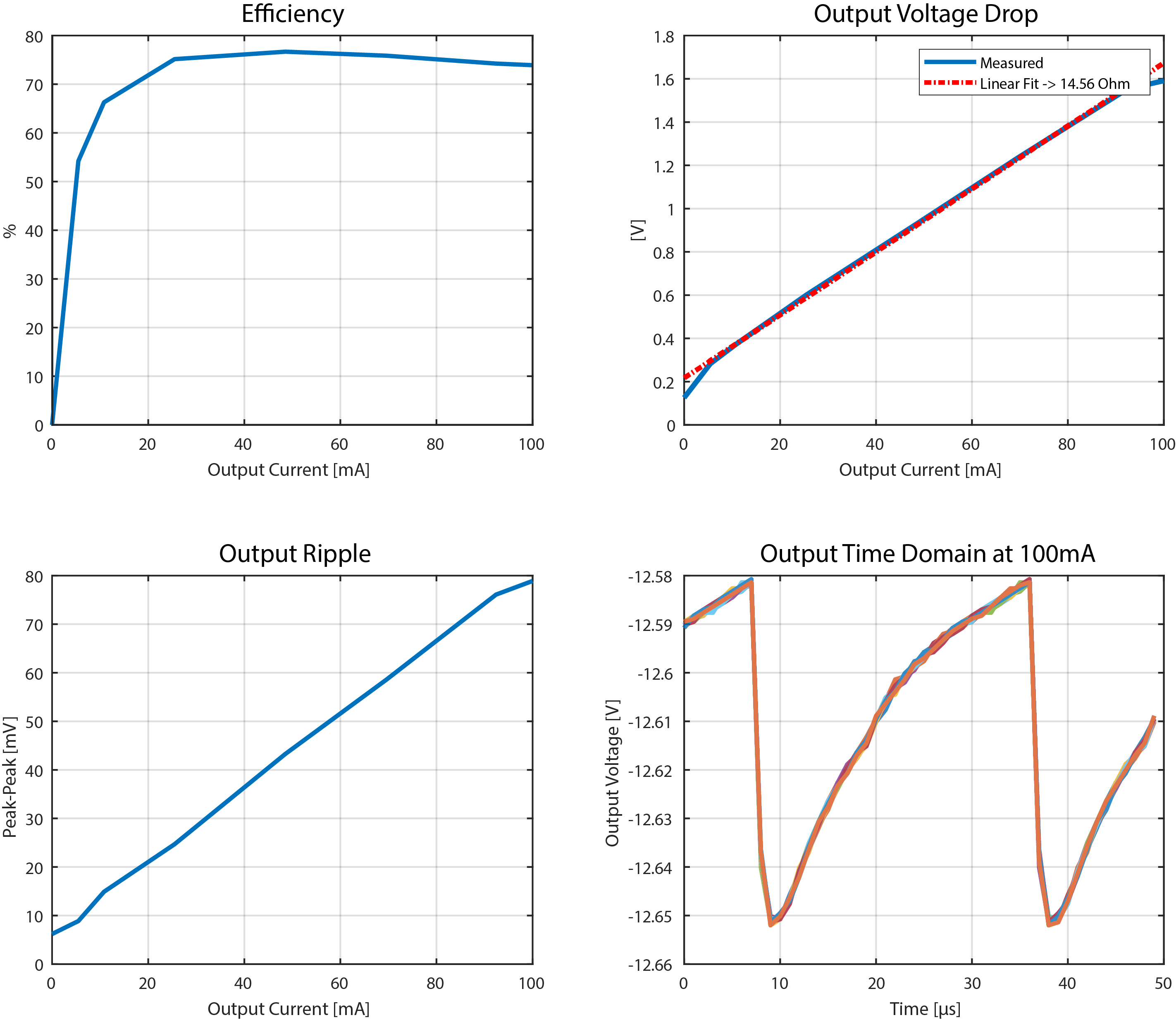
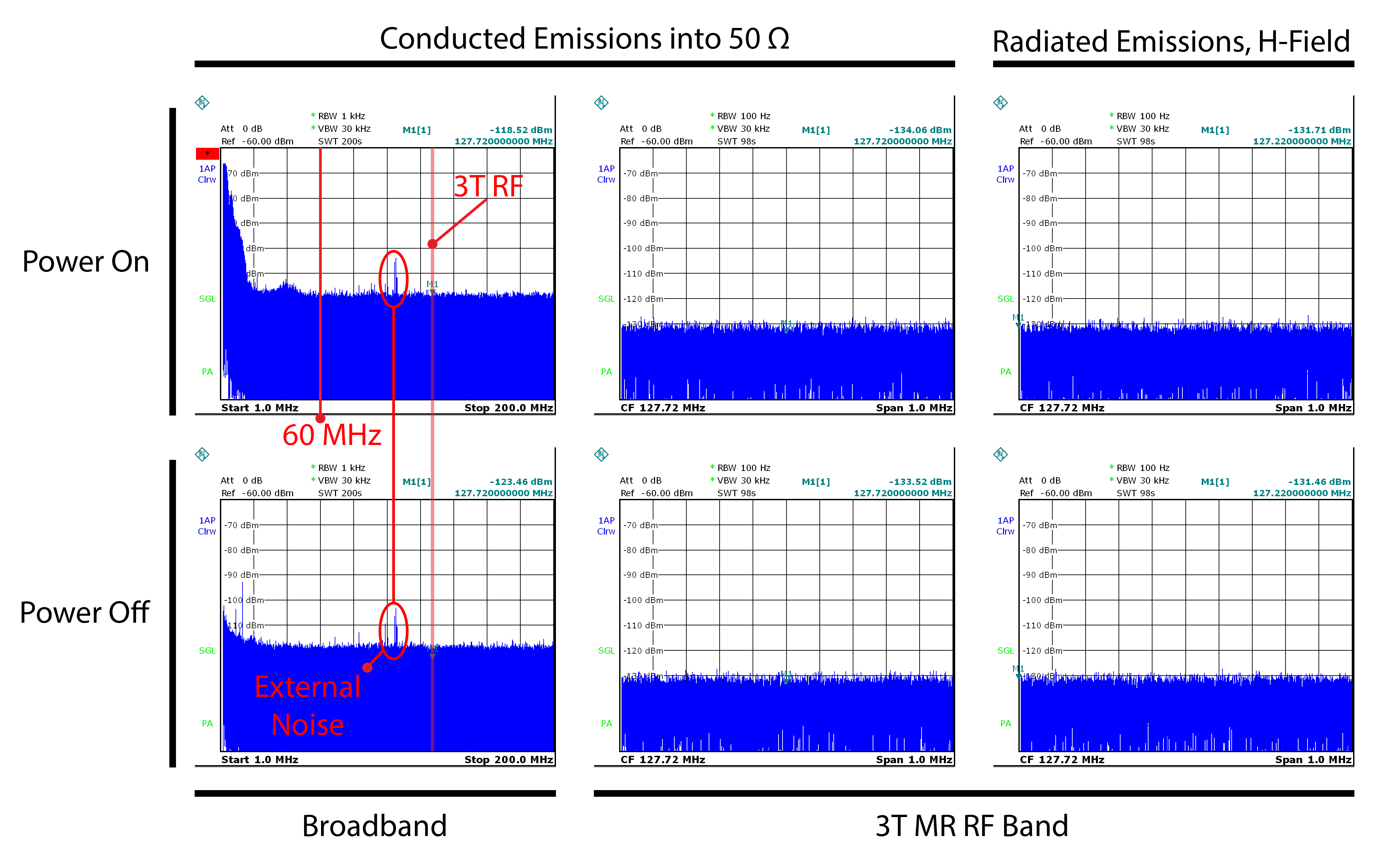
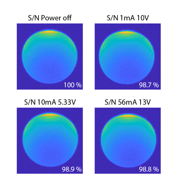
For implementing a switched capacitor inverter the operating principle shown in Figure 1 was chosen. A 10 µF ceramic capacitors (Cin) was used to pump charge to a 100 µF electrolytic capacitor (Cout). For implanting the switches and its auxiliary system a fully integrated IC was selected (LT1054, Texas Instruments, Dallas TX USA). Switching noise is blocked from the in- and output by passive filtering using ceramic SMD and feed-through capacitors. Key converter specifications such as efficiency, voltage drop and output ripple were measured load dependently (Fig. 3). Conducted (grid-bound) and radiated noise emissions were measured first on the bench (Fig. 4) by a spectrum analyser (FSL, Rhode&Schwarz) via a DC block and a pick-up loop respectively. Finally, the device was tested in a Philips Achieva 3T scanner (Philips, Healthcare, Best, Netherlands). The device was placed inside the standard 8-channel coil. As test load for the converter, a loop with a diameter of approximately 10cm was connected to the output using different series-resistors for load pulling. To sensitively detect potentially emitted noise the loop and the converter were located inside the MRI receiver array. The SNR of a standard GRE acquisition was compared depending on the operating state of the converter.Results
As shown in Fig. 3, the conducted emissions of the converter reside mainly below 20 MHz and are below the thermal level above 60 MHz. The noise spectrum below 20 MHz shows discrete peaks at the switching frequency (34.5 kHz) and its harmonics. The output ripple (Fig. 4) is a sawtooth wave and has correspondingly a spectral fall-off of 20 dB per decade. Furthermore, the output is attenuated at higher frequencies by the passive filtering adding another 20 dB per decade. In total, this matches the observed slope of 40 dB per decade below 20 MHz well. In the 3T MRI band (127.72 MHz, 1 MHz bandwidth) no measurable emissions, conducted or radiated, could be detected. The efficiency of the converter (Fig. 4 ) is around 75% for medium to high loads. The output voltage drop can be closely approximated as a 15 Ohm series resistor. The peak-to-peak output ripple follows roughly a linear relationship with Vpp = 0.75 mV/mA +6.1mV. The measurements in the 3T scanner (Fig. 5) does not show any additional noise picked up by the 8-channel head coil. The maximum measured SNR degradation was less than 1.5% in average over the volume compared to the case when the converter is turned off.Discussion & Conclusion
The presented converter is fully MR compatible without additional RF shielding nor requiring large inductances and delivers a comparably high efficiency. Similar results are expected for equivalent configurations for voltage multiplications or divisions instead of inversion. Many in-bore applications require low-current, negative or higher voltage rails as for example for PIN diode reverse or FET biasing. The converters can be simply parallelized to provide higher output currents as verified with up to five parallel converters capable of putting 500 mA out. Higher output current, efficiency and power density can be achieved by employing external switching transistors e.g. made from GaN substrates. In addition, capacitors with lower losses and higher capacitance densities e.g. based aluminium polymer technology are readily available. In applications requiring a higher output stability, the output ripple can be reduced by running at a higher switching rate or deploying a linear, low-dropout post-regulation. In conclusion, switched capacitor converters represent an interesting and broadly applicable alternative for biasing of in-bore MRI electronics.Acknowledgements
No acknowledgement found.References
[1] Vogt, C. (2017). Design Concepts and Validation of In-field MRI Electronics (Doctoral dissertation, ETH Zürich, Zürich, Switzerland). Retrieved from https://doi.org/10.3929/ethz-b-000246692
[2] Byron, K, Robb, F, Stang, P, Vasanawala, S, Pauly, J, Scott, G. An RF‐gated wireless power transfer system for wireless MRI receive arrays. Concepts Magn Reson Part B. 2017; 47B:e21360. https://doi.org/10.1002/cmr.b.21360
[3] J. G. Werthen, M. J. Cohen, T-C. Wu, S. Widjaja, Electrically Isolated Power Delivery for MRI Applications, Proc. Intl. Soc. Mag. Reson. Med. 14 (2006)
[4] M. J. Riffe, J. A. Heilman, and M. A. Griswold, Power scavenging circuit for wireless DC power, Proc. Intl. Soc. Mag. Reson. Med. 15 (2007)
Figures