RF Receivers: Signal Detection Chain, Digitization, System Noise Figures - from MRI Signal to Bits
1University of Alberta, Canada
Synopsis
This lecture covers the components of the RF chain from detection of the signal in the RF coil to its final representation as digital data. Each component is described and its effect on signal strength and quality is discussed.
Receive Chain Overview
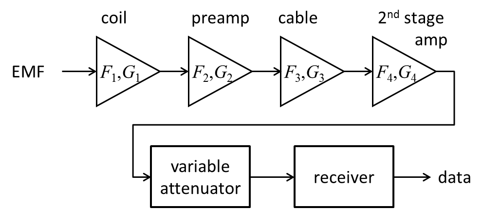
The receive chain (Figure 1) takes the small electromotive force (EMF) or voltage induced in the RF coil (or multiple coils in the case of arrays) and converts it into digital data for further processing into images, spectra, etc.Amplification
The receive chain must amplify small voltages induced in the coil to appropriate levels for the receiver’s input (approximately 1V). Signal levels in MRI are maximum at the center of k-space where the nuclear magnetization is in phase. A volume excitation (3D imaging) can induce a signal of approximately 10mV, while for single-slice excitation the signal could be 0.1mV, depending on slice thickness, and for spectroscopy much smaller still. At the edges of k-space, signals fall into the thermal noise, $$${V_n}=\sqrt{4kT\Delta fR}$$$, where $$$k$$$ is the Boltzmann constant (1.38×10⁻²³J/K), $$$T$$$ is the absolute temperature, $$$R$$$ is the coil resistance and $$$\Delta f$$$ is the bandwidth [1]. For a typical imaging sequence $$$\Delta f$$$=100kHz, $$$R$$$=1W, and $$$T$$$=300K, so the noise voltage $$$V_n$$$=41nV.
Gain
In these scenarios the minimum amplification, or gain, required to bring the signal up to 1V is 100=40dB in the case of volume imaging and 10000=80dB in the case of 2D imaging. Achieving this gain requires multiple stages, as well as a means of adjusting gain to the signal level encountered in a specific situation. The total gain is equal to the product (or sum in dB) of the gains of individual stages, in the absence of mismatches. This condition is satisfied for many RF gain blocks (RF ICs), but is rarely true for discrete transistors used in MR preamps.
Noise Figure
Each device in the receive chain degrades SNR by adding noise as described by the noise factor [2]
$$F={\left({\frac{{SN{R_{in}}}}{{SN{R_{out}}}}}\right)^2}\ge 1,$$
which expressed in dB is the noise figure: $$$NF = 10\log F$$$.
The coil is the first device that degrades the ideal, intrinsic SNR ($$$iSNR$$$) achievable with a lossless coil because of the noise generated by the coil’s resistance. This SNR loss is related to the loaded and unloaded quality factors ($$$Q$$$s) [3]
$$SNR=iSNR\sqrt{1-\frac{{{Q_{loaded}}}}{{{Q_{unloaded}}}}}.$$
Consequently,
$${F_{coil}}={\left({\frac{{iSNR}}{{SNR}}}\right)^2}=\frac{{{Q_{unloaded}}}}{{{Q_{unloaded}}-{Q_{loaded}}}}.$$
The noise factors of the devices in the receive chain do not add directly, but are scaled according to the amount of amplification in the preceding stages as stated by Friis’ formula [4]
$$F={F_1}+\frac{{{F_2}-1}}{{{G_1}}}+\frac{{{F_3}-1}}{{{G_1}{G_2}}}+\frac{{{F_4}-1}}{{{G_1}{G_2}{G_3}}} +...$$
where the respective noise factors ($$$F_i$$$) and gains ($$$G_i$$$) are labelled in Figure 1. The first stage of amplification must therefore have the lowest possible noise figure, typically $$$\le$$$0.5dB for the preamp, and $$$\le$$$1dB for the whole receive chain.
Linearity
Perfect linearity is impossible for arbitrarily large inputs, e.g., because the output amplitude of an amplifier is limited by its supply voltage. Nonlinear behavior leads to signal distortion such as intermodulation and compression, which is described by the power at which the output is reduced by 1dB (or 0.1dB for MR signals) relative to the ideal linear response. None of the devices in the receive chain must be allowed to reach compression under the strongest input signals.
Signal Transport and Attenuation
The receive chain must also transport signals (typically using coaxial cables) from inside the scanner bore to later stages of processing as far as several meters away in the equipment room. For optimal SNR a variable-gain amplifier or programmable attenuator is also needed so that the maximum signal in each scanning situation is near the maximum allowed at the input of the spectrometer. Cables and attenuators are described by the same parameters used for amplifiers:
- attenuation, or insertion loss, that is proportional (in dB) to the length of the cable, and
- noise figure, which is equal to the insertion loss [5].
Therefore, to preserve SNR the attenuator must be placed only after a large amount of amplification.
Receiver
The receiver converts the amplified RF signals (at frequencies near the Larmor frequency) to baseband (near zero frequency) digital data by performing demodulation and digitization (not necessarily in this order).
Demodulation
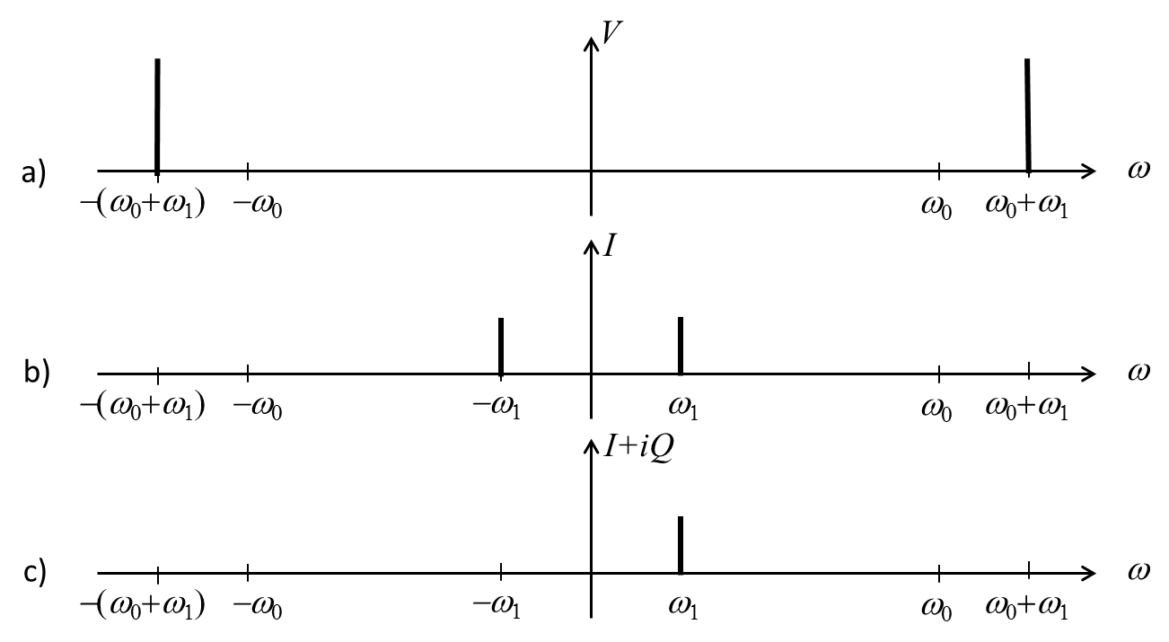
Signals in the rotating frame are more convenient to analyze because the high-frequency (RF) oscillations are eliminated by the process of demodulation. Because position in space is mapped onto frequency by the gradients, demodulation must preserve this transformation without introducing ambiguities like mapping multiple locations to the same frequency. A small voxel at location $$$x_1$$$ induces a voltage in the coil
$$V(t)\propto\cos\left[{\gamma({B_0}+{G_x}\cdot{x_1})t}\right]=\cos\left[{({\omega _0}+\gamma{G_x}\cdot{x_1})t}\right]=\cos\left[{({\omega _0}+{\omega _1})t}\right],$$
whose Fourier transform is shown in Figure 2a.
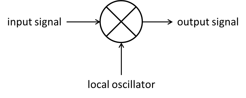
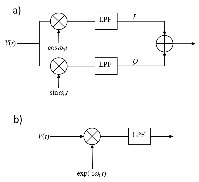
This spectrum, initially near the Larmor frequency, $$$\omega_0$$$, must be shifted down to DC by translating the frequency axis by this amount. One way is to use a product detector or mixer (Figure 3), which multiplies the incoming signal with a sinusoidal reference signal (at $$$\omega_0$$$) produced by the spectrometer (local oscillator).
Expanding using trigonometric identities,
$$I(t)=V(t)\cdot\cos{\omega _0}t=\cos\left[{({\omega _0}+{\omega _1})t}\right]\cos{\omega _0}t=\frac{1}{2}\left[{\cos{\omega_1}t+\cos(2{\omega_0}+{\omega_1})t}\right],$$
and the high-frequency component at $$$2\omega_0$$$ is removed by low-pass filtering (Figure 2b). Unfortunately, the same result is obtained if $$$\omega_1$$$ is replaced with $$$-\omega_1$$$ ($$$x_1$$$ is replaced with $$$-x_1$$$, or the gradient is reversed), therefore spatial locations $$$x_1$$$ and $$$-x_1$$$ cannot be distinguished, and the resulting image may be aliased. Quadrature demodulation (Figure 4), solves this problem by using a second mixer and a reference signal that is in phase quadrature with the other:
$$Q(t)=V(t)\cdot\left({-\sin{\omega_0}t}\right)=\cos\left[{({\omega_0}+{\omega_1})t}\right]\left({-\sin{\omega_0}t}\right)=\frac{1}{2}\left[{\sin{\omega_1}t-\sin(2{\omega_0}+{\omega_1})t}\right].$$
The two filtered outputs ($$$I$$$ and $$$Q$$$) are interpreted as the components of a complex signal and combined digitally, making the $$$-\omega_1$$$ component disappear as required (Figure 2c):
$$I+iQ=\cos{\omega_1}t+i\sin{\omega_1}t={e^{i{\omega_1}t}}.$$
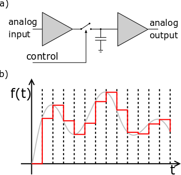
Digitization
Digitization converts the analog signal into a stream of digital data by performing discrete time sampling and amplitude quantization (often integrated in the same device). Sampling captures the values of a continuous waveform at discrete time points (Figure 5a), typically using a sample-and-hold circuit (Figure 5b). The Nyquist criterion applies, which states that the sampling frequency $$$f_s$$$ must be equal to or greater than twice the largest frequency component of the signal. The sampled values are fed to the input of an analog-to-digital converter (ADC) which assigns the voltage one of $$$2^b$$$ levels (where $$$b$$$=# of bits of the ADC) and then outputs this quantized level digitally. The quantization or rounding error can be modeled as white noise.
Acknowledgements
NAReferences
- JB Johnson. Thermal Agitation of Electricity in Conductors. Phys. Rev. 32(1): 97–109, July 1928.
- C.K.S. Miller, W.C. Daywitt, M.G. Arthur. Noise standards, measurements, and receiver noise definitions. Proceedings of the IEEE 55(6): 865– 877, June 1967
- W. A. Edelstein G. H. Glover C. J. Hardy R. W. Redington. The intrinsic signal‐to‐noise ratio in NMR imaging. Magn. Reson. Med. 3(4): 604–618, August 1986
- HT Friis. Noise Figures of Radio Receivers. Proceedings of the IRE 32(7):419–422, July 1944
- David M. Pozar, Microwave Engineering, Fourth Edition. 2012 Wiley.
Figures