1694
A Low Cost Prototype Pre-Gate Amplifier to Study Radiofrequency Power Amplification for Parallel Transmission MRI at 3 T1Physical Sciences, Sunnybrook Research Institute, Toronto, ON, Canada, 2Medical Biophysics, University of Toronto, Toronto, ON, Canada
Synopsis
There is a growing interest to increase the channel count on parallel transmit systems. With system cost always a major consideration, substantial savings may be possible as the channel count becomes high (ie. ≥32). Typically, radiofrequency power amplifier (RFPA) designs involve multiple amplification stages to achieve a target output power. Three stages are identified in the design approach of the present work: (1) a low noise pre-amplifier; (2) a driver amplifier; and (3) a power gain amplifier. The present goal is introduce and characterize system architecture for a prototype “pre-gate” amplifier (stage 1 and 2) to explore power amplification technology for stage 3 of the RFPA.
Introduction
There is a growing interest to increase the channel count on parallel transmit (pTx) systems. With system cost always a major consideration, substantial savings may be possible as the channel count becomes high (ie. ≥32). Radiofrequency power amplifiers (RFPAs) are often a major part of the expense but if the desired output power is distributed across a high number of channels, then use of mass production electronics (MPEs) becomes very attractive in terms of cost and hardware development time. Toward implementing a low cost high channel count pTx system at 3 T, therefore, it is important to investigate in-house RFPA designs that include MPEs. Typically, RFPA designs involve multiple amplification stages to achieve a target output power1-3. Three stages are identified in the design approach of the present work: (1) a low noise pre-amplifier; (2) a driver amplifier; and (3) a power gain amplifier. The present goal is introduce and characterize system architecture for a prototype “pre-gate” amplifier (stage 1 and 2) to drive the input gate terminal of the metal-oxide-semiconductor power amplifier. The prototype is an important preliminary step that will enable future investigation of the best design approach for the power amplifier (stage 3), including whether to use more common Double-diffused Metal Oxide Semiconductor (DMOS) technology, Laterally Double-diffused Metal Oxide Semiconductor (LDMOS) technology, or Gallium Nitride Semiconductor (GaN) technology.Methods
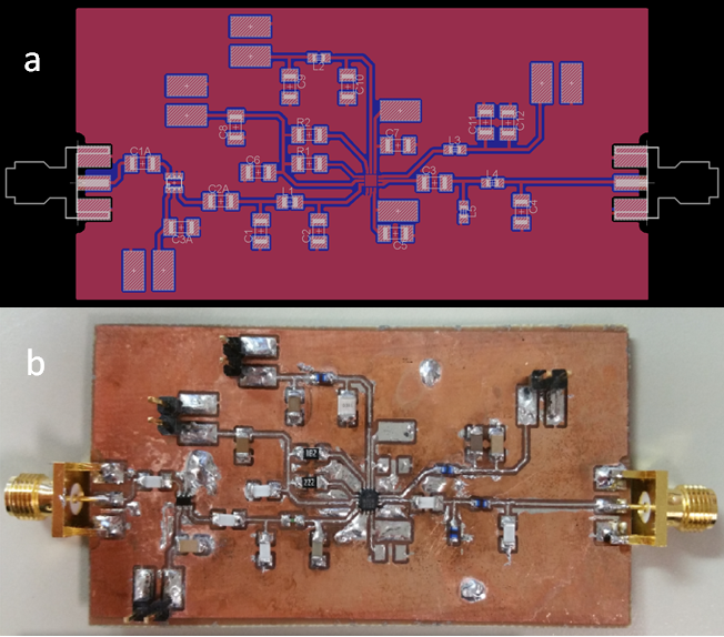
With the targeted system output power of 66 dBm (consistent with the 3 T Siemens Prisma for head applications) the estimated target per channel is 48-51 dBm for 32-64 channel pTx. The prototype is fabricated using NXP Semiconductor MPEs: a Silicon Monolithic Microwave Integrated Circuit (MMIC) wideband amplifier (BGA2867) for stage 1 and Heterojunction Bipolar Transistor Technology (InGaP HBT) (MMZ09332B) for stage 2. Figure 1 (a) shows the printed circuit board (PCB) layout designed in Eagle (Autodesk, San Rafael, CA) and (b) a photograph of the prototype, fabricated using photolithography.Results
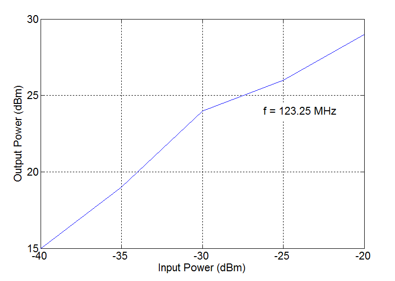
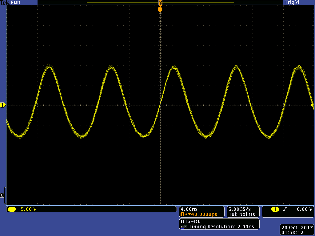
Bench measurements were taken using a network analyzer (E5061B, Keysight Technologies, Santa Rosa, CA) and a mixed domain oscilloscope (MDO-4104-6, Tektronix Inc., Beaverton, OR). The S11 (input return loss) and S21 (transmission gain) were measured as -16 dB and 54 dB, respectively, at the proton resonance frequency of 123.25 MHz (Siemens Prisma). Figure 2 shows a plot of the measured RF output power versus RF input power. The maximum measured output was 29 dBm. Figure 3 shows the RF output from a continuous input sine wave at 123.25 MHz.Discussion
The S11 and S21 results are consistent with the manufacturer specifications. Reasonable linearity and signal stability are observed in Figure 2 and Figure 3. The results are promising and demonstrate strong potential to drive candidate solutions for stage 3 of the RFPA. Although the maximum output power measured is 1 dB less than desired, this is easily resolved on the next design cycle. PCB design modifications (wider signal traces, better signal grounding and an improved heat sink) have commenced to improve signal reliability/isolation and heat dissipation concerns. The total bill of materials to assemble and manufacture this prototype was approximately $40 USD. The projected cost of for in-house manufacture of a complete RFPA prototype (a single channel pTx amplifier) is: (1) $140 – 200 USD for DMOS technology (DU2860U/DU28120T, MACOM, Lowell, MA); (2) $140 USD for LDMOS technology (MRF6V2150N, NXP, Eindhoven, NL); and (3) $250 USD for GaN technology (NPT2022, MACOM, Lowell, MA). The estimated costs only consider materials for RFPA operation and do not include functionality requirements for pTx integration (ie. RF blanking, safety monitoring, etc.). Costs can reduce considerably with higher order volumes of materials and outsourcing PCB manufacturing. Additional savings are possible with the future goal of incorporating a signal modulator and amplifier design into a single RF module4.Conclusion and Future Work
The work presented here demonstrates a promising device to investigate power amplifiers. Work has commenced to address the PCB issues observed during initial testing and the next step is to design and fabricate final stage prototypes and perform a full RFPA characterization. Future work includes MRI testing and prototyping a complete RF module.Acknowledgements
1. Canada Foundation for Innovation
2. Natural Sciences and Engineering Research Council of Canada
References
[1] Raab et al. “High-Efficiency RF Power-Amplifier Module for Magnetic-Resonance Imaging” ISMRM (2011)
[2] Chu et al. “Ultra-Low Output Impedance RF Power Amplifier for Parallel Excitation” MRM (2009)
[3] Twieg et al. “High Efficiency Radiofrequency Power Amplifier Module for Parallel Transmit Arrays at 3 Tesla” MRM (2017)
[4] Yang et al. “A Low Cost Signal Modulator for a Field Programmable Gate Array based Parallel Transmit System” ISMRM (2015)
Figures