1691
A Gate Modulated Digitally Controlled Modified Class-E Amplifier for On-Coil Applications in 1.5 T MRI1Department of Electrical and Electronics Engineering, Bilkent University, Ankara, Turkey, 2National Magnetic Resonance Research Center (UMRAM), Ankara, Turkey
Synopsis
A novel technique of modulating both the amplitude and frequency of the desired MR Radiofrequency pulse in a class-E amplifier topology, without utilizing supply-modulation, is presented. Amplifier’s MATLAB model is developed and the carrier frequency bitstream is intelligently controlled to achieve both the amplitude and phase modulation of the output waveform. Benchtop experiments are performed showing
Introduction
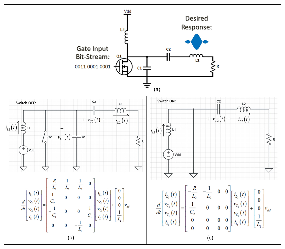
The conventional applications of class-E amplifiers require supply modulation where frequency and phase of the output waveform are controlled from the gate of the transistor while the amplitude is modulated from drain supply voltage1-3. In typical 50% duty cycle operation5 of the amplifier, the digital gate signal of the transistor can be considered as a uniform sequence of ones and zeros. Pulse width modulation (PWM) cannot be used in class-E topology since the system is non-linear. Delta-sigma modulation is another alternative. In this work, we utilize a combination of these techniques while considering the nonlinear behavior of the class-E amplifier, and modulate both the amplitude and frequency of the desired MR RF pulse by digitally controlling the gate signal of a transmission-line modified1 class-E amplifier, without the need for utilizing supply modulation, for on-coil excitation purposes in 1.5 T MR imaging [Fig.1(a)].Methods
Under the assumption of an ideal switch, the amplifier operation is broken down into two modes: switch-on and switch-off [Fig.1(b-c)]. State-space matrix representations for both these modes are written, from which the waveform equations are derived, and implemented in MATLAB.
The amplitude and phase of the output waveform are now modulated by digitally controlling the duty cycle and phase of the carrier frequency applied to the gate of the transistor. Working at f = 64 MHz, we associate each cycle (T = 15.625 ns) of the carrier frequency with k bits, where in our case, k = 4. An RF pulse of duration w = 2 ms would require a carrier signal of the same duration, consisting of $$$\frac{w}{T}$$$ cycles and consequently $$$n=\frac{k\times w}{T}$$$ bits. In order to achieve the desired pulse shape at the output, 2n combinations for the carrier frequency exist to choose from, requiring infeasible computational power.
At this point, the carrier bitstream is divided into multiple subsections. In each subsection, $$$k\times m$$$ number of bits (where m is an integer ranging from 1 to 16 and equals the number of cycles being controlled per each subsection) are controlled and repeated over the entire subsection (for m = 16, sampling rate equals $$$T\times m=0.25\ \mu s$$$ at 64 MHz, providing a bandwidth of 4 MHz), and the amplifier model is run for that subsection. A set of only three bitstream patterns {0000=0%, 0001=25%, 0011=50%} is used for controlling each cycle. The resulting output waveform for each subsection is compared in amplitude with the desired pulse for that subsection. Once the amplitude match is obtained, the bitstream elements are shifted left or right to achieve the phase match. This process is repeated for all subsections until a customized carrier bitstream, with least error between the desired and predicted waveforms, is generated.
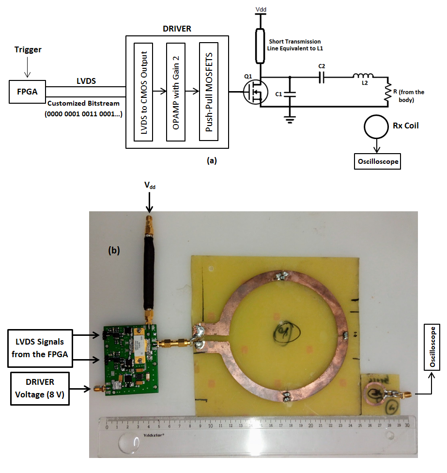
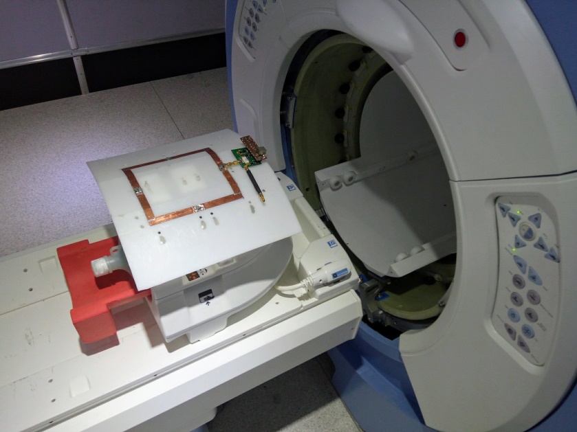
To test the validity of the technique, the generated carrier bitstream was tested on hardware setup similar to Ref-1 [Fig.2(a-b)]. MR experiments were conducted in 1.5 T (Scimedix Inc., Incheon, South Korea) MR Scanner to test the slice selective capability of the generated RF pulse (Fig.3).
Results
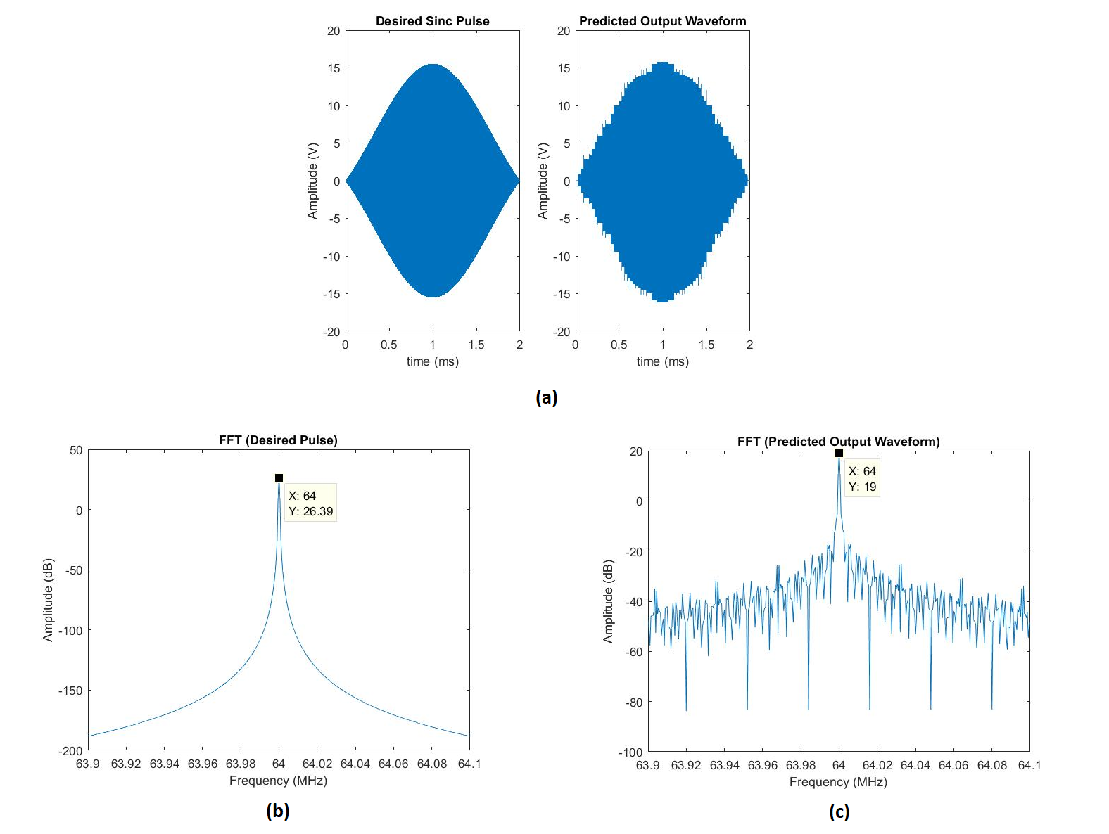
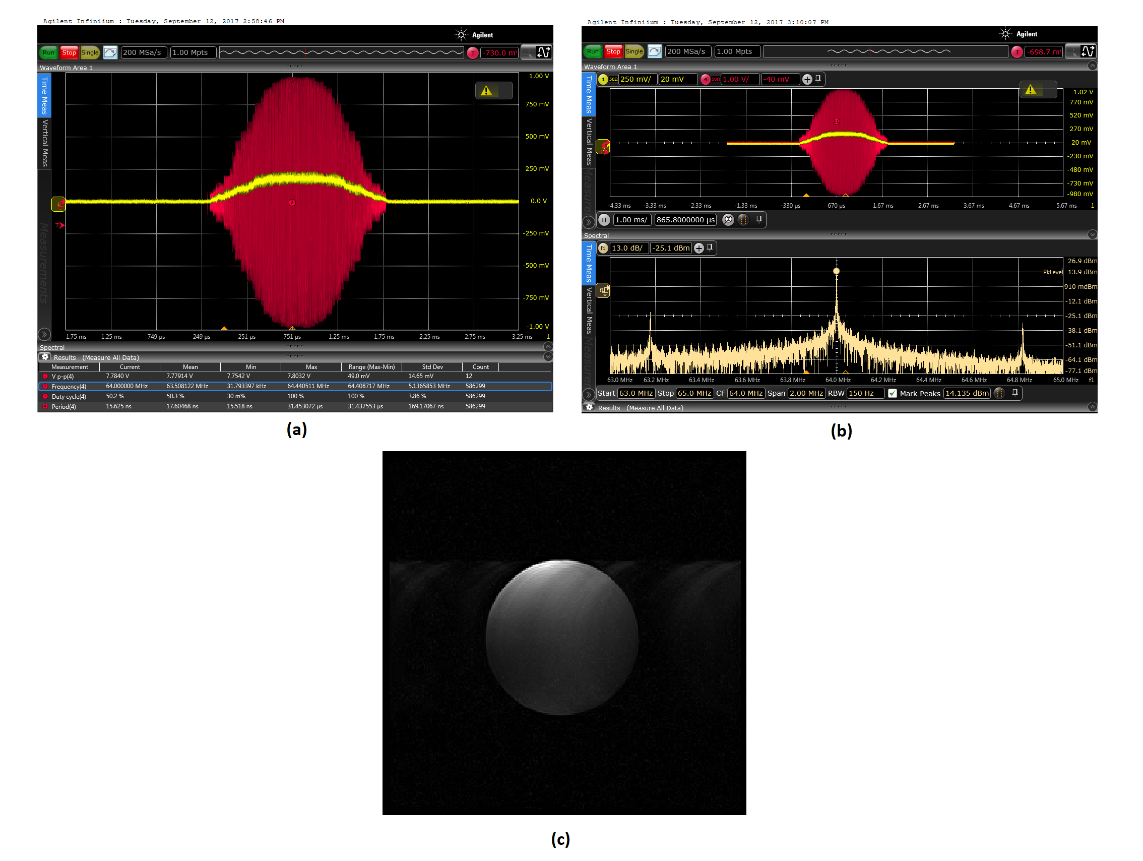
The desired and predicted output waveforms, along with their respective frequency spectrums, are shown in Fig.4(a-c). The maximum and root-mean-square errors between the desired and predicted output waveforms were calculated as 15.8% and 5.0% respectively. The output waveform and its frequency spectrum for benchtop experiments are shown in Fig.5(a-b). The peak drain efficiency for the amplifier was measured as 89%. The MR image is shown in Fig.5(c).Discussion
Since the MATLAB model assumes an ideal switch, a few of the quantization levels in the output waveform obtained in hardware do not match precisely with their software counterparts when software-optimized carrier bitstream is first implemented on hardware, hence requiring additional adjustments for a few subsections of the bitstream. The amplifier output power capability is 300 W, but the presented research is carried out till an output power of 80 W. Improvements in the system and algorithm are currently being worked on to achieve the goal of high output power capability while maintaining high efficiency at the same time. The ghosting artifacts observed in MR image are suspected to be associated with phase inconsistencies and synchronization problems which are currently being dealt with.Conclusion
A new technique of gate-modulating both the amplitude and frequency of the desired RF pulse is presented. The technique is general and can be implemented at higher field strengths as well, provided the system is tuned to that frequency and also the hardware is capable of transmitting bit-streams at higher rates. Using this technique, the overall cost of the system will decrease since the supply-modulation will not be required.Acknowledgements
No acknowledgement found.References
1. Poni, R., Silemek, B., Gundogdu, U., Demir, T., Ertan, N.K. and Atalar, E., Modified Class E Amplifiers Used For Two Channel Digital RF Transmit Array System With Integrated Coil, ISMRM, Singapore, 2016.
2. Zahra, F.T., Silemek, B., Poni, R., Ashfaq, B.N. and Atalar, E., A Highly Efficient 250 W Digitally Controlled Supply-Modulated Modified Class-E Amplifier for on-Coil Implementation in 1.5T MRI, ESMRMB, Barcelona, Spain, 2017.
3. Poni, R., MS.Thesis: A Digitally Controlled Class E Amplifier for MRI, Bilkent University, 2016.
4. Poni, R., Demir, T. and Atalar, E., A Digital Power Amplifier for 1.5 T, ISMRM, Toronto, Canada, 2015.
5. Sokal, N. O. and Sokal, A. D., "Class E-A New Class of High-Efficiency Tuned Single-Ended Switching Power Amplifiers," in IEEE Journal of Solid-State Circuits, vol. 10, no. 3, pp. 168-176, Jun 1975.
6. Sokal, N.O., Class-E High-Efficiency Power Amplifiers, from HF to Microwave, Proceedings of the IEEE International Microwave Symposium, Baltimore, June 1998.
7. Sokal, N.O., Class- E Switching-Mode High-Efficiency Tuned RF Microwave Power Amplifier: Improved Design Equations, Proceedings of the IEEE International Microwave Symposium, Boston, June 2000.
8. Gudino N, Heilman JA, Riffe MJ, Heid O, Vester M, Griswold MA. On-coil multiple channel transmit system based on class-D amplification and pre-amplification with current amplitude feedback. Magn Reson Med 2013;70:276–289.
9. Gudino N, Duan Q, de Zwart JA, Murphy-Boesch J, Dodd SJ, Merkle H, van Gelderen P, Duyn JH. Optically controlled switch-mode current-source amplifiers for on-coil implementation in high-field parallel transmission. Magn Reson Med 2016;76:340–349.
Figures