0950
Advanced Gradient Driver Design with Silicon Carbide MOSFETs1GE Global Research Center, Niskayuna, NY, United States, 2GE Global Research, Bangalore, India, 3GE Global Research, Niskayuna, NY, United States
Synopsis
In a MRI system, gradient driver is a switching power supply which is composed of power semiconductor devices, such as insulated gate bipolar transistors (IGBTs), power metal oxide semiconductor field effect transistor (MOSFET), etc. To control an electrical power that can be transferred by the gradient driver, the power semiconductor devices are usually operated in a pulse width modulation (PWM) method with high voltage, high current and high switching frequency [1-4]. With advanced semiconductor devices like silicon carbide devices, each module could sustain higher voltage which will simplify the power supply architecture. Meanwhile, the fast switching capability of Silicon Carbide (SiC) devices make the gradient amplifier more efficient than silicon version. This paper presented a high performance modular solution gradient amplifier system with advanced wide-band gap SiC devices. Image test with the advanced gradient driver was demonstrated in this paper.
Introduction
In a MRI system, gradient driver is a switching power supply which is composed of power semiconductor devices, such as insulated gate bipolar transistors (IGBTs), power metal oxide semiconductor field effect transistor (MOSFET), etc. To control an electrical power that can be transferred by the gradient driver, the power semiconductor devices are usually operated in a pulse width modulation (PWM) method with high voltage, high current and high switching frequency [1-4]. With advanced semiconductor devices like silicon carbide devices, each module could sustain higher voltage which will simplify the power supply architecture. Meanwhile, the fast switching capability of Silicon Carbide (SiC) devices make the gradient amplifier more efficient than silicon version. This paper presented a high performance modular solution gradient amplifier system with advanced wide-band gap SiC devices. Image test with the advanced gradient driver was demonstrated in this paper.Silicon Carbide (SiC) Gradient Driver
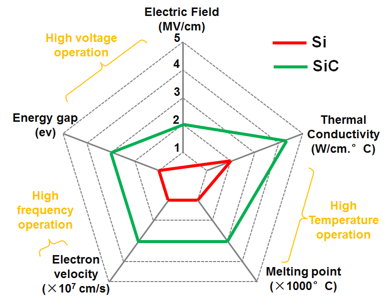
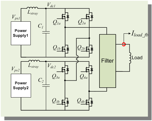
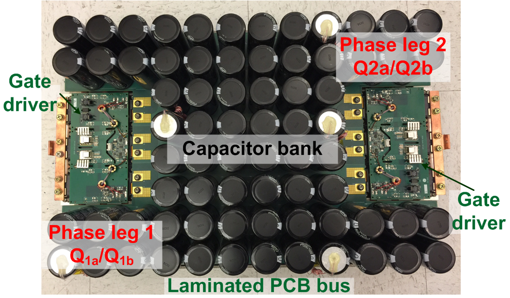
As indicated in Fig.1, the new wideband gap devices made of materials such as SiC provide a much higher bandgap, breakdown field, thermal conductivity which offer them the potential capability to overcome the frequency, temperature and power management limitations of traditional silicon devices. Fig.2 shows the improved two stages structure with high voltage (1700V) GE SiC MOSFETs. The modular structure brings the benefit of higher components volume, simpler implementation and lower lost. Fig.3 shows the fabricated one H-bridge prototype. PCB bus structure supported both power modules and bulky capacitors. Both power module and PCB bus low inductance design was performed to fully utilize the SiC fast switching capability. Each H-bridge input is 1350V and the total DC link voltage is 2700V. The capacitor bank is composed of distributed aluminum capacitors and total capacitance is selected based on energy storage requirement.Gradient Driver Power and System Test
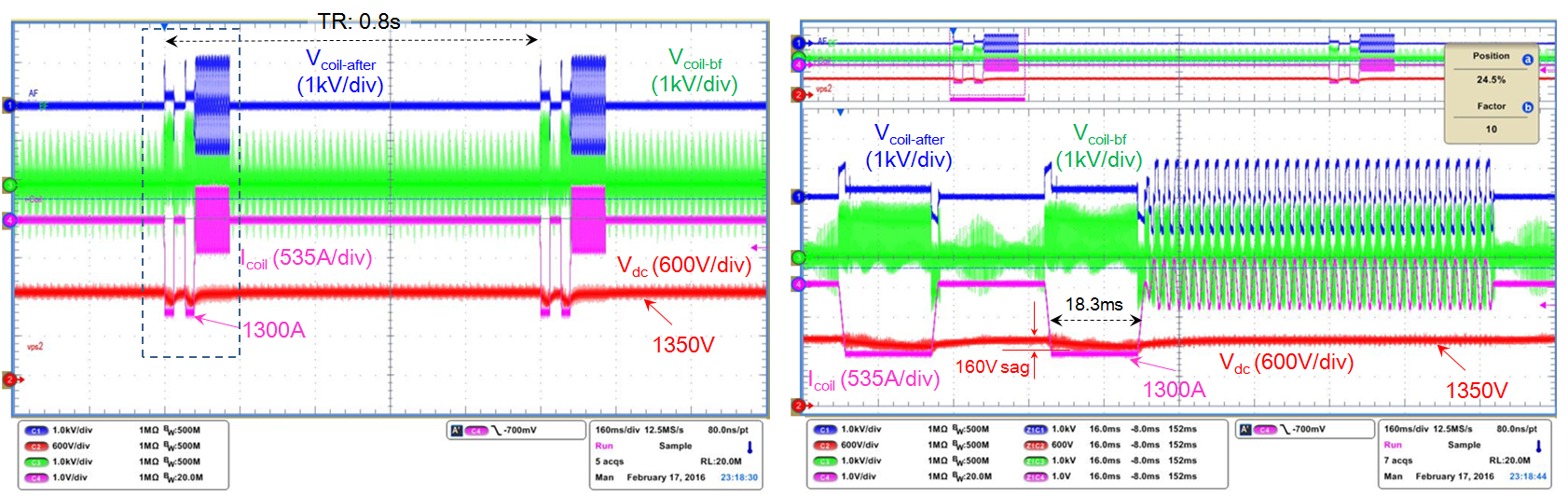
Two of the H-bridge shown in Fig.3 was utilized to build cascaded gradient driver as example. The gradient driver was first tested with pillar load around 900μH and the power test results are shown in Fig. 4. The switching frequency of the power module is 31.25kHz. An output filter was also designed and connected to the H-bridge output to filter out the high frequency harmonic before applying to the load inductor. The peak coil current is 1300A and the TR is controlled to be 0.8s to have 300A RMS current under this operating condition. The peak power delivered through this gradient amplifier exceeds 3.5MVA. The gradient amplifier power stage loss reduced to half at this operating condition compared with predicted silicon version gradient driver. The reduced loss will reduce the cooling system installation cost.
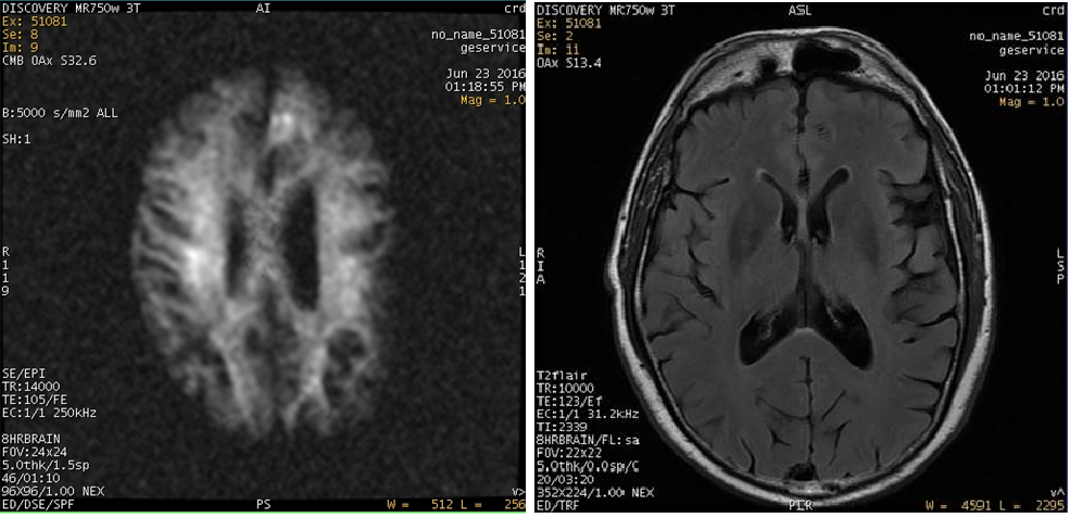
As shown from Fig.5, the developed prototype was installed and volunteer scan was performed on a 3T system. Fig. 5(a) shows test results with Diffusion Test and Fig. 5(b) shows the results with T2 Flair test.
Conclusion
In this paper, the gradient amplifier power stage design with only two stages cascaded structure was demonstrated. GE 1700V SiC devices were selected and the system design was optimized with low parasitic to fully utilize the SiC device fast switching capability. The maximum power rating with this design exceed more than 3.5MVA peak power. This design enables lower loss with simple architecture which will reduce the cooling system installation cost and the modular solution will also enable lower engineer and implementation cost without sacrificing the high bandwidth and high-power capability.Acknowledgements
No acknowledgement found.References
[1] A. Gupta, IEEE Trans on Power Electronics pp: 1672-1681, 2007. [2] R. Wang, et al., Pittsburg, ECCE, 2014. [3] F. Wang, et al., IEEE Trans on Industrial Application. pp. 1336-1341, 2000. [4] J. Sabate, et al., Proc. ISMRM. 2007Figures