4342
An open source waveform generator based on PulSeq for matrix coils1Department of Radiology, University Medical Center Freiburg, Freiburg, Germany, 2Faculty of Engineering, University of Freiburg, Freiburg, Germany
Synopsis
An open source waveform generator based on Pulseq (open-source pulse sequence programming environment) for emerging matrix coils was developed, with the channel count of up to 64. The FPGA development board integrated with USB3.0 is used to store the waveform data and generate the waveform in real-time when external trigger signal is activated. The generator software was written in Python 2.7 with a queue structure.
Introduction:
Matrix coils, also known as multi-coils, using multiple coil elements, were developed for shimming to improve the magnetic homogeneity and for encoding to generate customized spatial encoding magnetic fields1-3. To generate multi-channel waveforms, one solution is to use an FPGA controller to store the current waveform into the local memory ahead of the experiments, controlled by a custom pulse sequence software4. An alternative is to use the commercial high-speed digital IO board to generate current waveform in real-time with an open-source pulse sequence programming environment, Pulseq5,6. To make the published Pulseq-based solution completely open source, here we present the adapted design of the waveform generator with up to 64 channels.Methods:
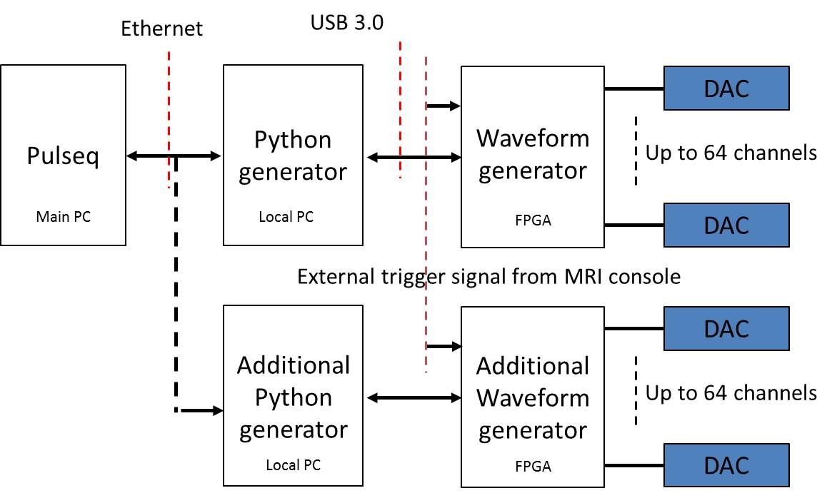
A block diagram of the waveform generator is shown in Fig.1. The Pulseq console is used to define the high-level pulse sequence and is extended to simultaneously control the additional amplifier channels and the Siemens system for RF pulses, traditional gradients and signal acquisition. A waveform file for the additional gradient channels is sent to the local PC. The generator software was written in Python 2.7 using PyCharm (JetBrains, Praha, Czech Republic). The Python script loads the waveform file, and then interprets these files to meet the data format requirement of the FPGA board. Since the Pulseq data file contains no loops but a simple list of instructions, the memory requirements might become impractical when channel count is high, especially for long sequences. To address this, a queue structure was implemented in Python script to periodically download new data when the data request is activated. The FPGA development board integrated with USB3.0 (XEM6310-LX45, Opal Kelly, Portland, USA) is used that stores a part of the current waveform in the local memory ahead of the experiment and reloads the new waveform data in real-time from local PC during the experiment. When called upon by the external trigger from Siemens console, the FPGA rapidly reads the current waveform data and applies them to the individual DACs via a high-speed serial interface, and requests new waveform data from local PC until the end. To synchronize the generator with the Siemens console, an external 10MHz reference clock from the Siemens console is used. Additionally, an interface board provides the galvanic isolation between FPGA board and DACs board via optical fiber.
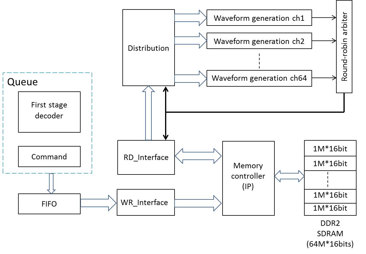
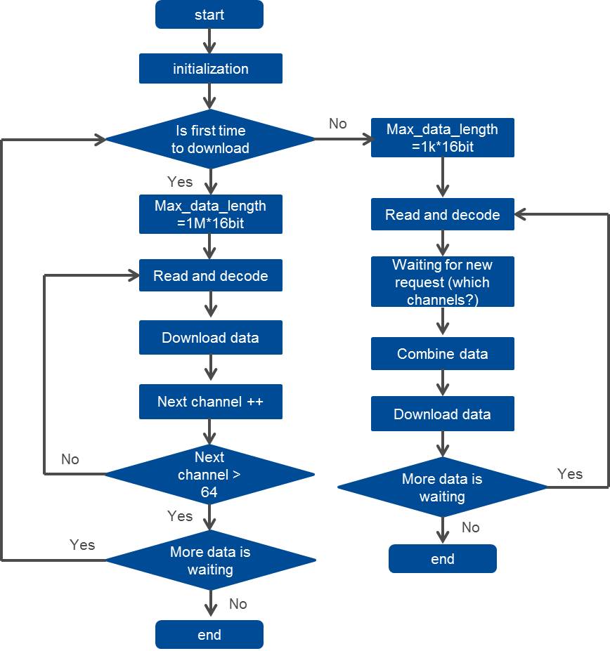
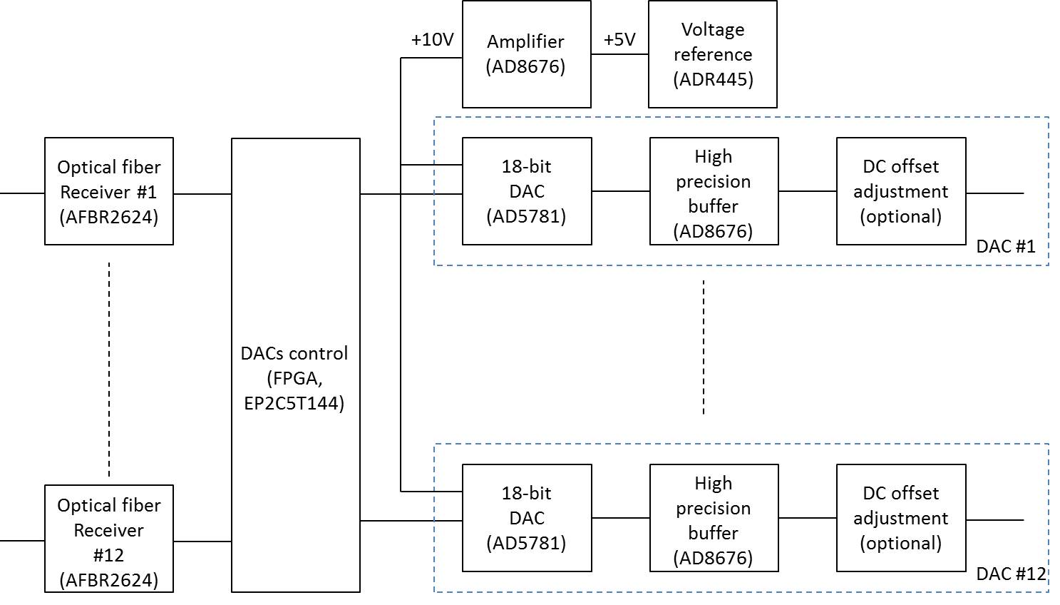
The block diagram of FPGA core module is presented in Fig. 2. The data is firstly buffered in a FIFO. Then the write-interface transfers the buffered data from the FIFO to DDR2 RAM via the memory controller. The read-interface loads the data stored inside the DDR2 RAM to the embedded FIFO of each channel via the distribution module. When the external start trigger is activated, each waveform generation channel will start to generate waveform simultaneously. The Round-Robin arbiter supplies the channels that need new data without starvation . Fig. 3 shows the flow diagram of the Python script with a queue structure. The block diagram of DACs board with up to 12 channels is presented in Fig. 4. The DACs board based on a high precision 18-bit DAC (AD5781, Analog Devices, Norwood, USA) converts the digital waveforms to meet the input requirements of power amplifiers. An optical fiber receiver (AFBR-2624, Avago technologies, San Jose) converts the optical fiber signal to the TTL signal. The field-programmable gate array (FPGA) implements the initialization of DAC and the waveform transfer. The AD5781 is governed by a high precision voltage reference (ADR445, Analog Devices, Norwood) with low noise and drift (2.25uVp-p 0.1-10Hz, and 1 ppm/°C). The output of AD5781 is buffered by an ultra-precision operational amplifier (AD8676, Analog Devices, Norwood, USA) with low noise and offset (0.1uVp-p 0.1-10Hz, and 12uV). The AD5781 provides a ±10V full scale output to match the input requirement of the currently used amplifier. An optional output offset adjustment circuit is incorporated to compensate for a possible DC voltage offset.
Discussion:
Although the present system can drive up to 64 channels, because of the scalability of the Ethernet, duplication can permit an order of magnitude increase in channel count without any hardware redesign. The waveform generator can be directly used or easily adapted for any analog-input shimming or gradient amplifier. Compared to the published generator, the cost of the present system is decreased four times. To further decrease the cost, the optical fiber can be replaced with optocoupler without sacrifice in galvanic isolation.Acknowledgements
This work is supported by the European Research Council Starting Grant ‘RANGEmri’ grant agreement 282345.References
1. Juchem C, et al., NMR IN BIOMEDICINE (2015); 2. Jia F, et al., Proc. ISMRM23 (2015), 3091; 3. Littin S, et al., Proc.ISMRM23 (2015), 1022; 4. Nixon TW, et al., Proc.ISMRM18 (2010), 1532; 5. Yu H., Proc. ISMRM24 (2016), 3548; 6. Layton KJ, et al., Magn Reson Med 2016, DOI 10.1002/mrm.26235Figures