4321
PIN-diode switched dual-tuned RF coils1Institute of Neuroscience and Medicine - 4, Forschungszentrum Juelich, Juelich, Germany, 2Current Address: Medical Physics in Radiology, German Cancer Research Centre (DKFZ), Heidelberg, Germany, 3Faculty of Medicine, Department of Neurology, JARA, RWTH Aachen University, Aachen, Germany
Synopsis
In this work we investigate the transmit and receive performance of a probe employing such switching, using a simple loop coil tuned to 45 and 169 MHz for the detection of 23Na and 1H, respectively, at 4T. PIN diode switched-capacitor networks work well under forward bias, but perform poorly in reverse bias. Specifically, a high reverse bias voltage is required to allow operation over a realistic range of RF transmit voltages. This makes such switched-capacitor networks unsuitable for use in transmit probes. However, they can be used in receive-only probes, because the voltages present on the loop are much smaller.
Purpose
PIN-diode controlled RF switches were recently proposed as a method to double-tune an RF probe for MRI/S, actively switching the resonance frequency between two different Larmor frequencies by adding or removing capacitors from the resonator circuit1,2. In this work we investigate the transmit and receive performance of a probe employing such switching, using a simple loop coil tuned to 45 and 169 MHz for the detection of 23Na and 1H, respectively, at 4T.Methods
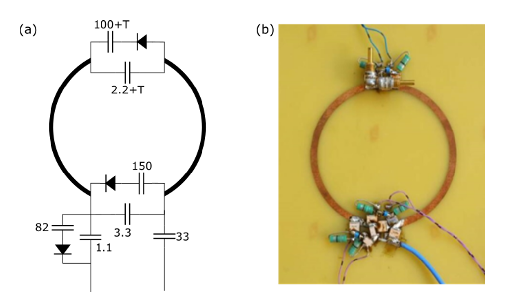
A loop was etched from PCB (80 mm inner diameter, 4.55 mm track width, 1.6 mm FR4, 35 μm Cu). Two PIN-diode switching units were added to the loop, and one to the matching network (Fig 1). MR measurements were carried out on a 4T home-assembled Siemens whole-body scanner using a cylindrical phantom (110 mm diameter, 100 mm long, axis vertical) containing distilled water, 45 mmol/L NaCl and 4.7 mmol/L NiSO4. The coil was connected to the scanner via a home-built dual-tuned T/R switch. Biasing for the diodes was provided by a bench power supply. Transmit performance was characterised using an oscilloscope via a sniffer loop during the MR experiment. The sniffer loop was positioned approximately 60mm below the coil on the coil axis. Fully-relaxed FID acquisitions (512 spectral points, 4 kHz spectral width, 10 averages) were made over a range of forward (10-150 mA) and reverse (0-100V) bias conditions. For each bias condition the transmit pulse amplitude was increased from 5-100V for 23Na and 1H, and the magnitude of the measured pulse amplitude was recorded. Receive performance was then characterised using a series of 3D flash (23Na) and GRE (1H) images over a range of forward (10-150 mA) and reverse (10-100V) bias conditions. For each bias condition, transmit pulse amplitude was measured again using an oscilloscope with sniffer loop. When the measured pulse amplitude was 2.35V for 23Na and 118mV for 1H, the signal-to-noise ratio (SNR) was calculated from 3D flash image for 23Na and GRE image for 1H. Note that sniffer loop was connected to oscilloscope through the -30 dB attenuator during the 1H experiment.Results
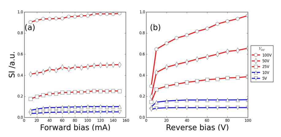
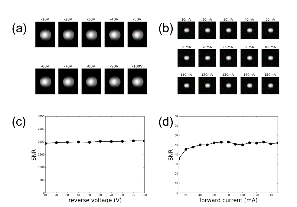
Figure 2 shows the measured pulse amplitude of the transmit signal plotted against the forward bias current/reverse bias voltage applied across the PIN diodes. When the diodes are forward biased (Fig. 2a, 23Na), the measured pulse amplitude shows a small linear increases with bias current. Under reverse bias (Fig. 2b, 1H), the measured pulse amplitude rapidly increases with reverse bias voltage from 5-10V. At lower transmit voltages (1-10V) the signal intensity then reaches a plateau. At higher transmit voltages the signal intensity continues to increase across the whole range of tested reverse bias voltages. Figure 3a,b shows 1H GRE images with different reverse bias voltages and 23Na 3D Flash images with different forward bias currents. Under reverse bias, the RF transmit voltage had to be increased at lower bias voltages to maintain a constant measured pulse amplitude. However, the SNR was almost the same over a range of reverse bias condition (Fig. 3c). Under forward bias, the system RF transmit voltage and the SNR show a slight increase with bias current (Fig. 3d).Discussion
When reverse biased beyond 10V, the measured pulse amplitude is independent of transmit voltage at lower transmit voltages (1-10V), as expected. At higher transmit voltages (25-100V), the measured pulse amplitude increases continuously across the whole range of tested bias voltages, indicating that the PIN-diodes are insufficiently reverse biased. PIN-diodes are sufficiently reverse biased when the bias voltage is greater than the RF voltage across them. When the PIN-diodes are insufficiently reverse biased, the RF transmit signal brings the diodes into partial conduction slightly detuning the RF probe. This also tends to dissipate excessive energy in the diodes, leading to component failure. Note that the system-supplied bias current/voltage for driving PIN-diodes is 100 mA/30V. While this is sufficient to drive PIN-diode switches in the forward condition, it places an unrealistic limit on transmit voltage in the reverse condition (<10V).Conclusions
PIN-diode switched-capacitor networks work well under forward bias, but perform poorly in reverse bias. Specifically, a high reverse bias voltage is required to allow operation over a realistic range of RF transmit voltages, far higher than typical system-supplied bias voltages, and often in excess of the reverse breakdown voltage of the PIN-diodes. This makes such switched-capacitor networks unsuitable for use in transmit probes. However, they can be used in receive-only probes, because the voltages present on the loop are much smaller.Acknowledgements
No acknowledgement found.References
1. HA, Seunghoon, et al. A PIN diode controlled dual-tuned MRI RF coil and phased array for multi nuclear imaging. Physics in medicine and biology, 2010, 55.9: 2589.
2. LIM, Heeseung, et al. Construction and evaluation of a switch-tuned 13C-1H birdcage radiofrequency coil for imaging the metabolism of hyperpolarized 13C-enriched compounds. Journal of Magnetic Resonance Imaging, 2014, 40.5: 1082-1090.
Figures