2694
High Power TRASE PIN Diode Control System1Electrical and Computer Engineering, University of Alberta, Edmonton, AB, Canada, 2Medical Physics, Cross Cancer Institute, Edmonton, AB, Canada, 3Oncology, University of Alberta, Edmonton, AB, Canada
Synopsis
TRASE is a k-space encoding method for low cost MRI that replaces conventional imaging gradients with a switchable RF transmit array. TRASE echo train sequences require rapid switching between transmit elements to cycle through up to six different phase gradient encoding fields. In vivo image resolution is currently limited because long (~500μs) refocusing pulses render the echo train sequence vulnerable to T2 losses. Here we present a design for a high power PIN diode driver circuit capable of robust and rapid switching of short (~100μs) high power pulses for a 24cm coil. Results from 0.2T experiments are shown.
Purpose
TRASE is a promising encoding technique for low cost MRI systems that replaces conventional gradients with a switched RF array1-3. The pulse sequence requires rapid switching of transmit coil elements, implemented by means of PIN diode enable / disable circuitry. TRASE employs RF phase gradients to effect progressive k-space encoding along echo trains. Short refocusing pulse length is crucial to imaging performance to keep echo train length within practical T2 times. Previous work has employed 500μs to 800μs RF pulses; the aim of this study is to reduce this to 100μs by improved design of the PIN diode switching sub-system leading to higher coil efficiency. Success would result in clinical-level spatial resolution.Technical Aims
Specific aims:
1. To achieve 100μs 180° pulse length for a 8.2MHz 24cm 1D TRASE Helmholtz-Maxwell coil3. (Biot-Savart calculations show this requires 59A.)
2. Minimal loss of Q due to insertion of diode circuit (ON state)
3. A robust OFF state, i.e. preservation of diode reverse bias when other transmit elements (unavoidable inductively coupled) are transmitting
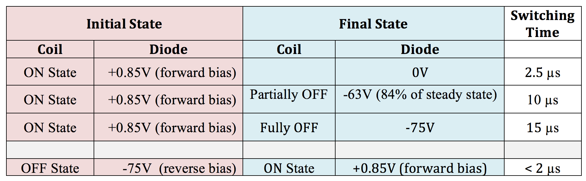
4. 5µs switch ON time; 10µs switch OFF time.
5. Compact lightweight design suitable for low cost, low power MRI systems
Methods
A PIN diode driving (PDD) circuit was designed to fit on a 13.5cm x 7.5cm PCB, with one fiber optic input and 4 outputs. For the switch (Fig.3) a MACOM MA4PK2000 PIN diode was selected; this is rated for 1MHz to 100MHz operation, with maximum series resistance of 0.2Ω (specified at 4 MHz), and maximum current of 25A (RF and DC). Caveat: the long carrier lifetime (30µs), can lead to slower switching.
MOSFET Push-Pull Switch: The design consists of two power MOSFETs that are switched with opposing states5. The MOSFETs are forced into either triode mode when the gate-source voltage is 15V, or cutoff at 0V. The first transistor switches a 48V power supply that drives a PIN diode load in forward bias with up to 580mA. The second transistor switches a negative voltage supply (-75V) for reverse biasing. Up to four diode circuits can be driven in parallel; each channel has a series 82Ω to limit the output to 580mA and reduce the RL time constant (τ = L/R seconds) for faster forward bias switch-on speeds.
Power System: The main power supply is a 48V 4.6A wall adapter DC supply (21cm x 7.3cm x 3.9cm), capable of powering up to 4 PDD units. The negative voltage supply is implemented using four isolated DC-to-DC converters. The use of integrated circuit DC-to-DC converters allows for a compact lightweight design. Additional fiber optic control was implemented as a safety precaution to disconnect all high voltages, when in the idle state.
NMR experiments were performed at 0.2 Tesla (8.2 MHz) to measure the 180° pulse length for the 24cm TRASE 1D phase gradient coil3 with diode circuitry installed.
Results
A low power bench test was performed to determine the RF voltage that appears across a given tuning capacitor for a given coil input power (also confirmed by ADS 2016 simulation[6]). The resulting estimate was 960W RMS input power required to produce 59A. Switching speed results are given in Fig.5. A bench power test was performed to evaluate the reliability of the Helmholtz transmit element. The coil can run 400W RMS pulses at 20% duty cycle for 30 minutes without arcing, or solder melting. Heating of capacitors causes a downward resonant frequency shift, which however stabilizes after 1 minute, and so was compensated for by pre-tuning the coil 15.7kHz high. NMR tests (at low duty cycle) of flip angle showed that for a square pulse the 180degree condition was reached for 180μs at 361W RMS; 100μs at 940 W RMS (during the pulse).Discussion
Next steps will be to upgrade other components (power splitter and phase shifter) for high power and perform high duty cycle and imaging tests using the shorter pulse lengths. Operation at kW levels requires management of power, voltage and thermal stresses. The driver system is fully expandable, with up to 4 driver boards stackable and driven by a single 48 V supply. Although not discussed here, due to the low operating frequency (8 MHz), SAR issues are comparatively minor.Conclusions
TRASE imaging is dependent upon precise control of the B1 transmit field in time and space, which in turn involves spatial and temporal control of high RF power systems. Progress has been made in the implementation of 100μs pulses, which is an important step towards feasible clinical applications.Acknowledgements
Department of Oncology, University of Alberta; Department of Electrical and Computer Engineering Coop Program, University of Alberta; Faculty of Veterinary Medicine, University of Calgary.References
1. Sharp, J.C., King, S.B MRI using radiofrequency magnetic field phase gradients Magn. Reson. Med. 63(1) 151-161, 2010.
2. Sharp, J.C., King, S.B. Deng, Q. Volotovskyy, V. Tomanek, B. High-resolution MRI encoding using radiofrequency phase gradients NMR in Biomedicine 26(11), Nov 2013, Pages 1602-1607
3. Deng, Q, King, S.B., Volotovskyy V., Tomanek B., Sharp J.C.; B1 transmit phase gradient coil for single-axis TRASE RF encoding Magn. Reson Imag. 31(6), 891–899 (2013)
4. Stockmann, J.P , Cooley, C.Z, Guerin, B., Rosen, M.S, Wald, L.L. Transmit Array Spatial Encoding (TRASE) using broadband WURST pulses for RF spatial encoding in inhomogeneous B0 fields. J. Magn. Reson. Vol 268, 1 July 2016, Pages 36-48
5. Xiao Y, Zhao Z, Qian, Z, Zhou, H. 2010 A high isolation switching unit for MRI system; Procedia Engineering 7 (2010) 265-269
6. Keysight - Advanced Design System (ADS) 2016
Figures
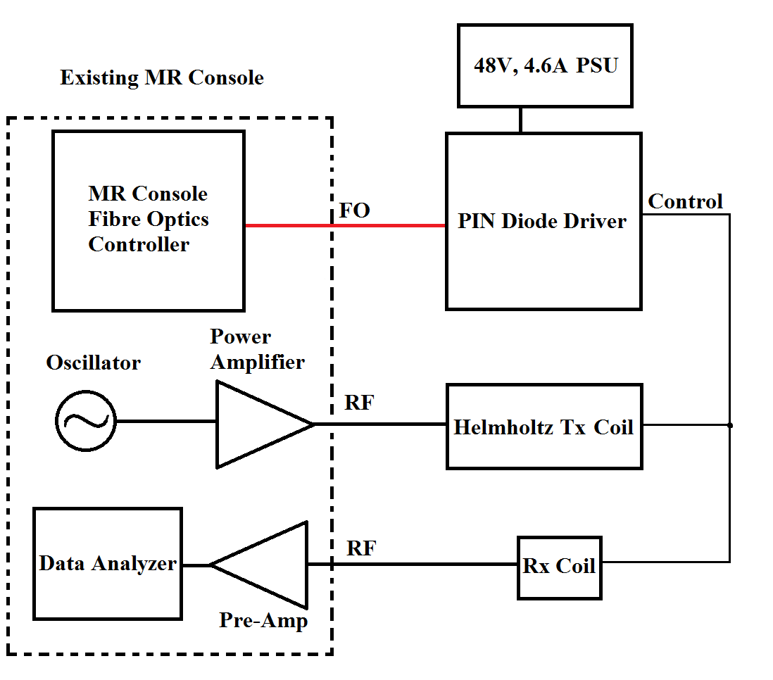
Figure 1. System Block Diagram. The PIN diode driver is interfaced to the MR console via fiber optic cables. The driver switches the PIN diode in the disable circuits of the transmit coil and the receive coil respectively.
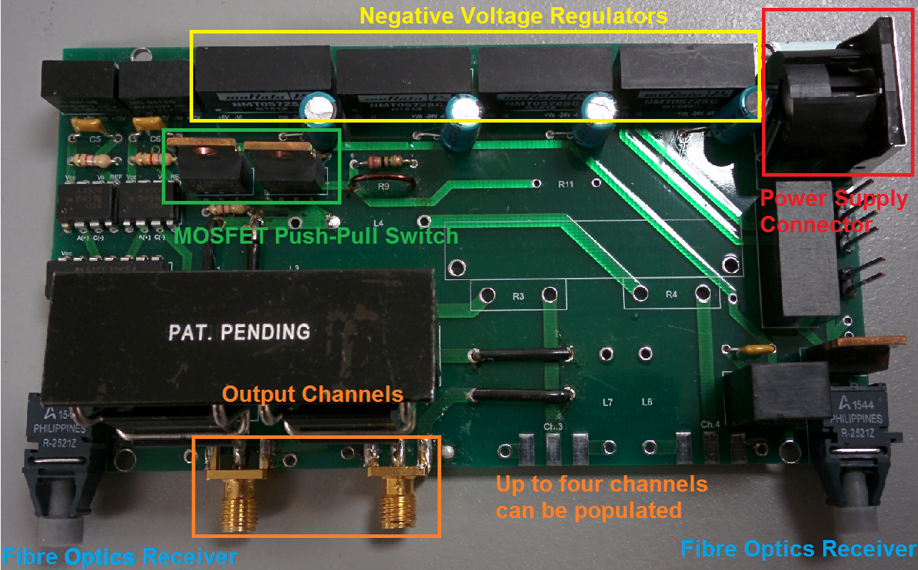
Figure 2. Photograph of PIN Diode Driver Board.
The diode drivers are controlled by fiber optics signals to prevent the transmission of electrical noise into the magnet room. Each driver board has two power MOSFETs which act as switches to either switch on a positive voltage to generate a forward bias current or a large negative voltage to thoroughly reverse bias the PIN diodes. Up to four output channels can be populated on the diode driver, controlled by a single fiber optic control signal. The diode driver board dimensions are 13.5cm x 7.2cm.
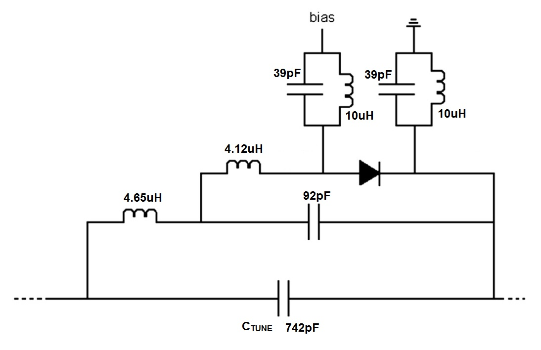
Figure 3. Diode Disable Circuit Schematic.
When the PIN diode is reverse biased, the 4.65µH inductor in series with the 92pF capacitor forms a resonant RF trap with the tuning capacitor on the Helmholtz transmit coil and disables the coil. When the PIN diode is forward biased, the 4.12µH inductor forms a resonant RF trap with the 92pF capacitor; the coil is in its on state when the diode is forward biased. The circuit was adapted from Deng et al 2013, some redundant capacitors in the network have been removed.
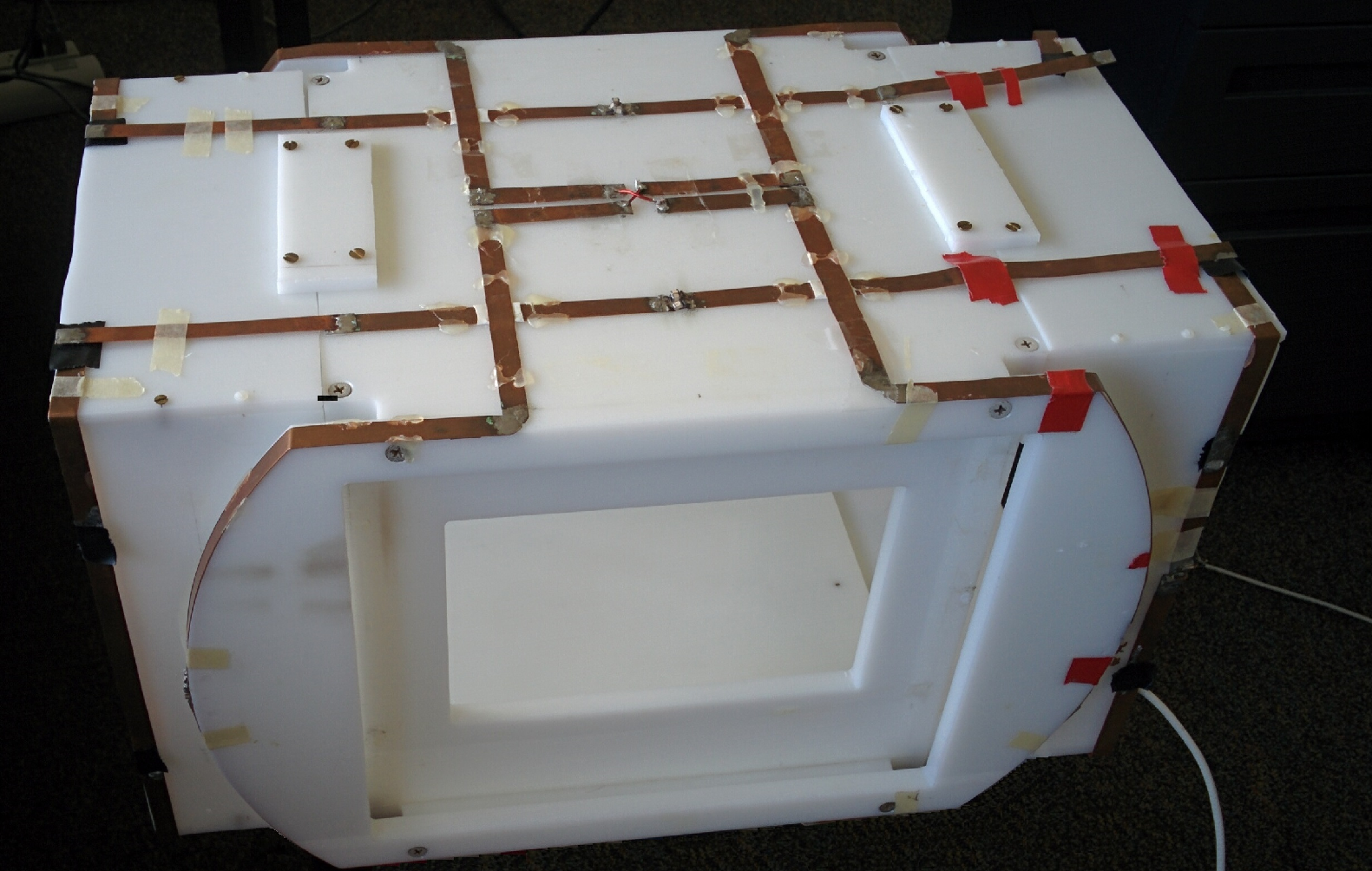
Figure 4. Photograph of the TRASE Transmit Array.
The photograph shows the 1-D Helmholtz-Maxwell TRASE transmit array used in this study. The average spacing of the coil conductors (coil i.d.) in the imaging volume is 24cm. This 2-element array may be driven either in-phase or out-of-phase to produce either a positive or negative phase gradient. See Ref 3.