1056
Correction of Gradient Induced Clock Phase Modulation for In-Bore Sampling Receivers1ETH Zuerich and University of Zuerich, Institute for Biomedical Engineering, Zuerich, Switzerland
Synopsis
With increasing receive channel counts, moving digitizer electronics close to the coil is desirable for reduced cabling and cable coupling and improved patient safety. However, gradient induction degrades in-bore operated circuit performance. Particularly vulnerable are high quality sampling or mixing clocks, required for digitization or demodulation. Gradient induced oscillator modulations add to the already stringent jitter requirements and therefore directly reduce SNR. We present a method which corrects large parts of clock modulations and therefore increases phase SNR of in-bore acquired data e.g. 18 dB for a sinewave corrupted by EPI gradients.
Introduction
Since the advent of parallel imaging methods, MRI spectrometers with increasing channel numbers are in demand. The recent trend for adding additional sensors in-bore, such as for field monitoring, aggravate this requirement1.
Scaling channel counts poses challenges in managing the required cabling and raises severe handling issues. For improved patient safety and signal integrity it is thus beneficial to move digitizer electronics close to the coil.
Several implementations of this effort have been presented, ranging from wireless transmission2 to complete in-bore spectrometers3 or on-coil digitizers4.
A common requirement to all digitizer approaches is the presence of a precise clock, as the dynamic range and signal-to-noise ratio (SNR) is majorly determined by the phase noise of the clock providing either the local oscillator for downconversion or the ADC sampling clock for direct conversion5. Jitter becomes the dominant source of signal degradation at high input frequencies as encountered with modern ultra-high field systems.
Transmission of precise clock signals can be hampered by RF interferences when guided galvanically and by added jitter when using optical transmission. Similarly, local (in-bore) clock signal generation is difficult particularly due to gradient induced voltages, resulting in clock drifts and distortions.
Here, we present a method to resolve these
problems by deploying a local (in-bore) low noise clock generator which is
phase locked to an external reference for stability and synchronicity. Erroneous
phase modulations induced by reference spurs and gradient induction on the
digitized data are compensated by feeding back the effectively applied sampling
clock to the host system, where its additional jitter is measured, for real-time correction of acquired data.
Methods
Sampling clock phase modulations and the consequent timeline misplacement ($$$g_{∆t}$$$) of acquired signal samples $$$s_\tau(n)=s(nT+g_{∆t}(nT))$$$ at rate $$$1/T$$$ can be corrected for by simultaneously measuring phase deviations of the affected clock ($$$\phi_{clk}$$$) and time re-positioning digitized samples either in real-time or in a post processing step by phase addition (Fig.1).
$$$s_{corr}(n)= s_\tau(n)\cdot e^{-i 2\pi f_{in} g_∆t(nT)}=s_\tau(n)\cdot e^{-i\phi_{corr}(n)}$$$ with $$$g_∆t(nT)=\frac{\phi_{clk}(n)}{2\pi f_{clk}}$$$ gives $$$\phi_{corr}(n) = 2\pi f_{in}g_∆t(nT)=\frac{f_{in}}{f_{clk}}\cdot\phi_{clk}(n)$$$
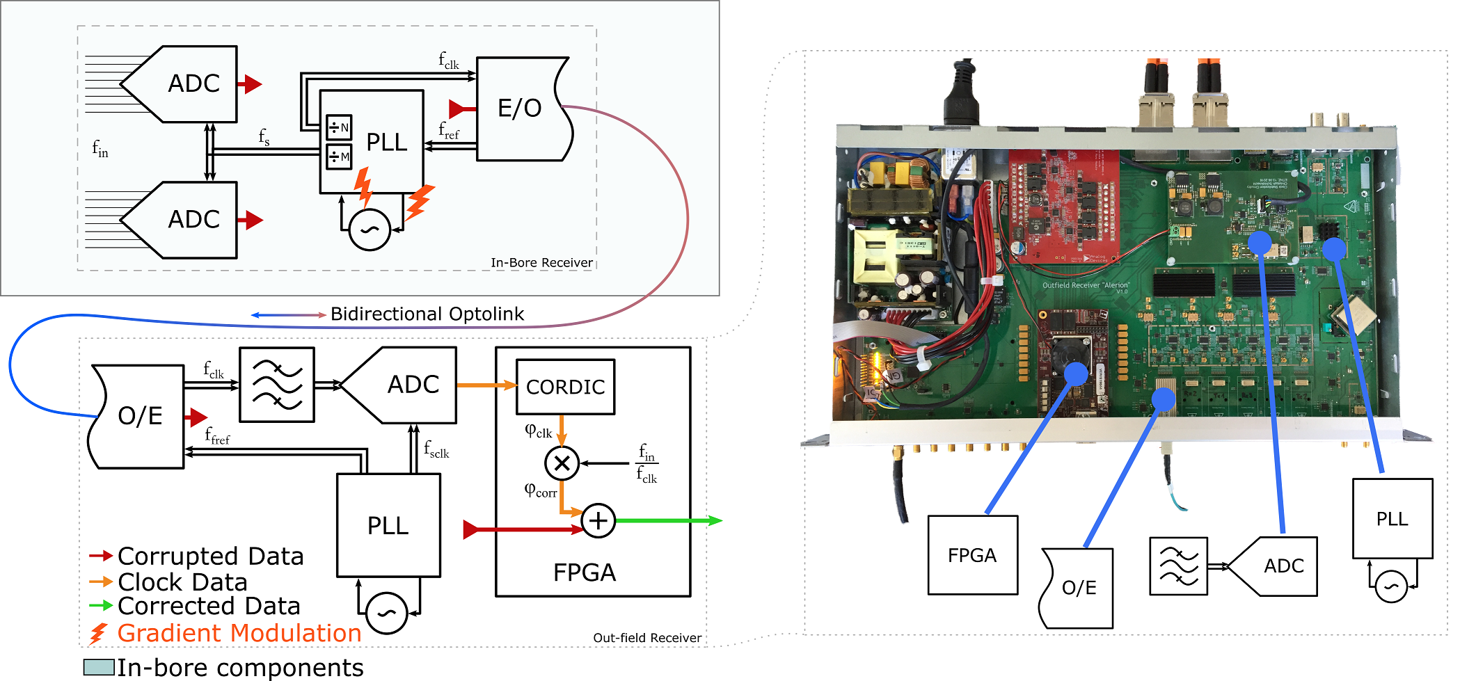
Hardware Setup
A 500MHz reference clock is fiber-optically transmitted from the console to the in-bore clock circuitry, where a PLL cleans the received clock from noise added by the optical link. The derived ADC sampling clock is then together with the acquired data (16 ADC channels) retransmitted back to the reference system. The fed-back clock signal is band pass filtered and digitized at 156.25MSPS (LTC2107, Linear). The acquiring FPGA (Z7045, Xilinx) demodulates, decimates, filters and extracts its phase. Finally, the clock phase is time aligned and added to the phase of the incoming data streams in real-time.
Experiments
Results were obtained from measurements on 7T
and 3T scanners (Philips Healthcare, NL). The in-bore receiver was placed on the patient bed (40cm from the iso-center) and test signals (295MHz/7T
and 130MHz/3T, SMA100A Rhode&Schwarz) were acquired while different gradient
sequences were played out, including sinewave, EPIs and Spirals with various
gradient slew-rates and orientations.
Further, EPI and Spiral trajectories were
monitored using a 16-channel field camera, connected to the in-bore receiver.
Results
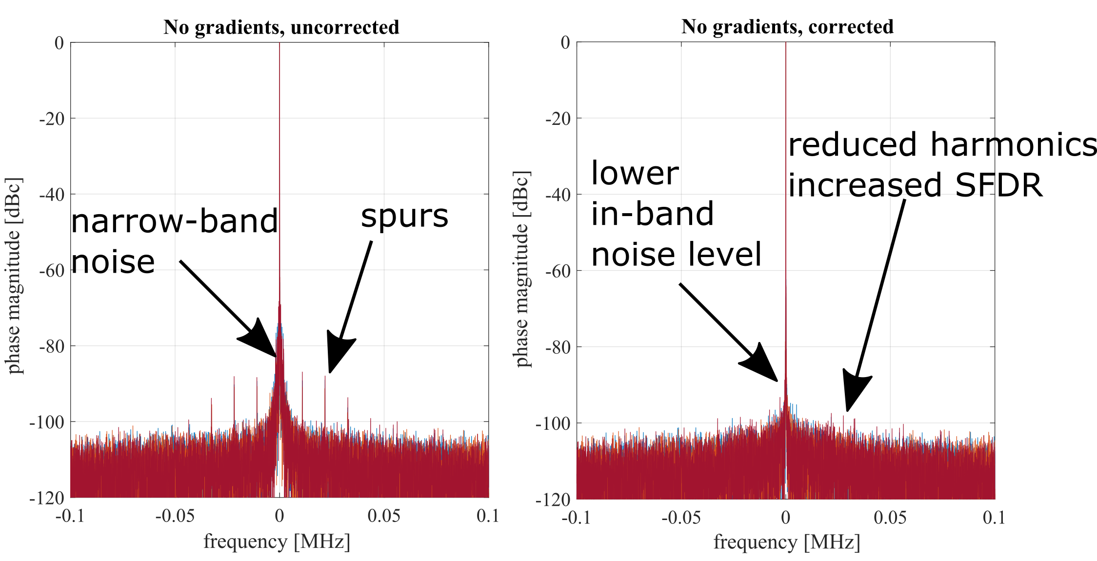
The clock phase measurement hardware exhibited a phase noise floor of 0.58mrad rms at 500MHz input (equiv. 185fs). Without the clock feedback, the dynamic range of the in-field receiver is limited by narrow-band noise and spurs induced by the local in-field clock (Fig.2). These are removed by the clock feedback approach, increasing the overall SFDR by 16dB and strongly reducing narrow-band noise.
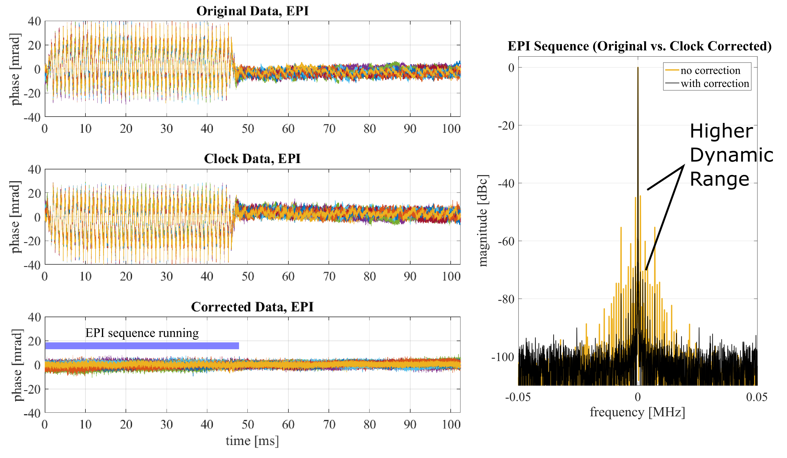
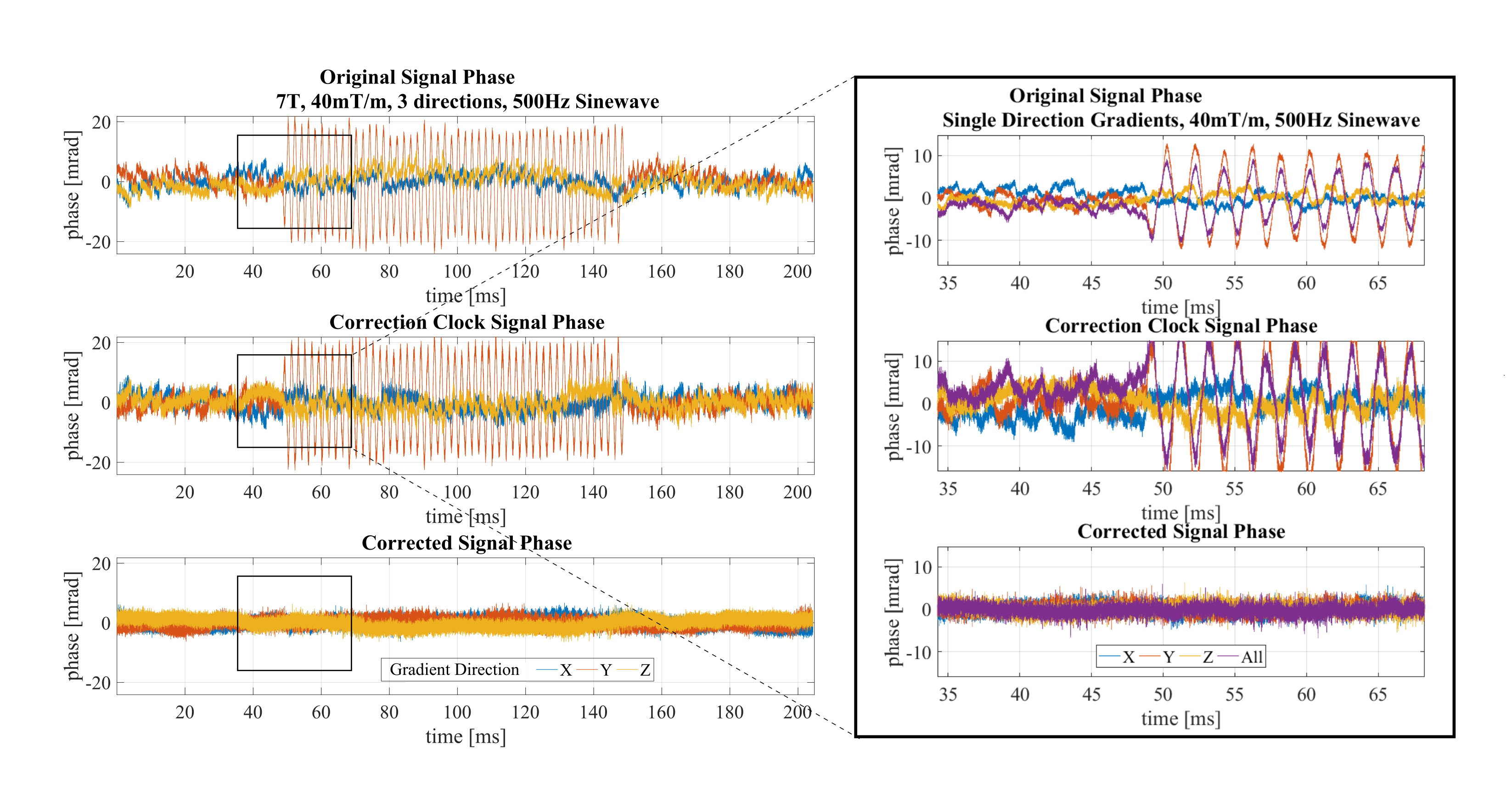
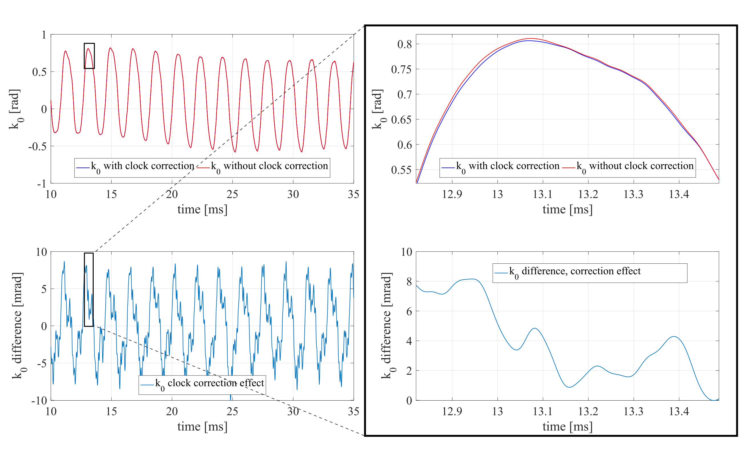
Under an EPI sequence with full gradient duty-cycle, phase distortions of up to 40mrad were induced in the local reference clock signal (Fig.3). For comparison, such a clock phase error would create a corresponding EPI ghosting image of up to 4%. Using clock feedback the phase distortions are corrected down to the noise floor of the receiver, resulting in an rms phase SNR improvement of 17.9dB. Even with strongest available gradients (200mT/m/s, 40mT/m) the influence of gradient induction on the magnitude of the signal was in the worst case 10ppm only.
Discussion and Conclusion
The presented method was shown to effectively remove spurs and noise originating from imperfections of local clock sources used on in-bore digitizers which is required to leverage the performance of roday's analog converters. Thereby the advantage of full synchronicity provided by an up-link reference clock is combined with the robustness and accuracy of a down-link based system. Also, phase drifts induced by the optical link itself can be detected since the clock signals run in the same physical fiber. These advantages make the presented approach ideal for synchronizing multiple receiver modules and other system components with tight timing constraints.Acknowledgements
No acknowledgement found.References
1. Dietrich BE, Brunner DO, Wilm BJ, Barmet C, Gross S, Kasper L, Haeberlin M, Schmid T, Vannesjo SJ, Pruessmann KP, "A Field Camera for MR Sequence Monitoring and System Analysis", Magn Reson Med. 2016 Apr;75(4):1831-40
2. Aggarwal K, Joshi K, Rajavi Y, Taghivand M, Pauly J, Poon A, Scott G., "A Millimeter-Wave Digital Link for Wireless MRI", IEEE Trans Med Imaging. 2016
3. Reber J, Marjanovic J, Brunner DO, Schmid T, Moser U, Dietrich BE, Barmet C, Pruessmann KP, "In-Bore
Broadband Array Receivers with Optical Transmission", Proc. Int. Society Magn Reson Med., 2014, pp. 0619
4. Sporrer B, Bettini L, Vogt C, Mehmann A, Reber J, Marjanovic J, Brunner DO, Burger T, Pruessmann KP, Troster G, Huang Q, "Integrated CMOS receiver for wearable coil arrays in MRI applications", IEEE DATE 2015, pp. 1689-1694
5. Arkesteijn VJ, Klumperink EAM, Nauta B, "Jitter Requirements of the Sampling Clock inSoftware Radio Receivers", IEEE Trans Circ Sys; 2006 Feb;53(2):90-94
Figures