1600
High Resolution PWM Generation for High Frequency Switching Gradient Amplifier Control1Aselsan A.S., Ankara, Turkey, 2Electrical-Electronics Engineering, Bilkent Universitesi, Ankara, Turkey, 3National Magnetic Resonance Center, Bilkent Universitesi, Ankara, Turkey
Synopsis
Recently gradient array systems draw attention of researchers with their capabilities. However, it is crucial to drive all array elements as desired to be able to spoil all the advantages of the gradient array. In terms of adjusting the timing of the gradient pulses, generating pulse width modulation (PWM) signals from one source, i.e. a single FPGA, for all array amplifiers would be a good solution. However, required number of bits to generate PWM signal would be limited to clock frequency. In this abstract, required digital resolution to generate PWM signals is analyzed and a method to generate PWM signals with resolution less than using I/O delay (IODELAY) elements of virtex7 family FPGA is presented.
Introduction:
Recently gradient array systems draw attention of researchers with their capabilities1,2. However, it is crucial to drive all array elements as desired to be able to spoil all the advantages of the gradient array. In terms of adjusting the timing of the gradient pulses, generating pulse width modulation (PWM) signals from one source, i.e. a single FPGA, for all array amplifiers would be a good solution. However, required number of bits to generate PWM signal would be limited to clock frequency. In this abstract, required digital resolution to generate PWM signals is analyzed and a method to generate PWM signals with resolution less than using I/O delay (IODELAY) elements of virtex7 family FPGA is presented.Methods:
To determine the required resolution simulations were done using the parameters shown in Table 1. Systems maximum gradient value was defined as Hz/m to perform generic simulations instead of using a specific gradient coil and current value. As $$$ V(t)=R_{coil} i(t)+ L_{coil} \frac{\text{d}i(t)}{\text{d}t} $$$ current on the coil have linear relationship with the applied voltage. Assuming an ideal switch mode amplifier, digitization in the PWM signal will be linearly mapped to the gradient coil current. Also, as the Biot Savart law is used for calculation of the gradient field from the applied current, any digitization error in the current will be linearly mapped to the gradient field. So during the simulations digitization error induced on the gradient value. A circular phantom with radius 20mm was used in simulations and signal equation was calculated for gradient echo with 20msec echo time. Required gradient values calculated for 1.28msec flat time for readout and 2msec for phase encode gradients, fall and rise times were 300usec for both and phase encoding gradient was digitized sweeping the number of bits from 9 to 16. Although required gradient can be corrected by changing the duration of the gradients, digitization would also impose limitations to timing so the digitization error only added to magnitude of the gradient pulse. During simulations RF excitation was not considered and a spin in x direction was assumed at the beginning of each TR. Error in the images were defined as $$$|I_{original}-I_{digitized} |/avg(I_{original})$$$ and calculated pixel by pixel. Also an error term was defined for gradients as $$$∫_0^τ|(G_{coil}-G_{desired})|dt $$$ where is the gradient duration and maximum error through the simulation was calculated for number of bits from 9 to 18. After defining the required bits for PWM, center aligned PWM signal generation was tested using VC707 evaluation board. 200MHz onboard clock was used in FPGA clock wizard IP core to generate synchronized 400MHz clock signal which will be used as main counter for PWM signals. To achieve higher resolution IODELAY elements of the high performance pins of the FPGA was used. A 5 bit counter was used for IODELAY elements which are counted with the clock $$$ 1 ⁄ (200MHz⁄(2 ×2^5 ))≈78psec$$$. Duty cycles of PWM signals for each carrier period were calculated on a computer and clock and IODELAY counters for the transition points of PWM waveform were found. PWM waveforms were calculated to feed the full bridge amplifier, such that the difference between right and left legs is equal to the calculated duty of the original PWM. In Figure 1 calculated values are shown for one leg of the full bridge. a is the clock counter value and b is the IODELAY counter value. a and b values for two transition points of PWM signals were calculated as shown in Figure 1. These values were written to block ram on the VC707 board and applied to high performance output of the FPGA by reading from the ram. Generated signals were simulated using model sim.
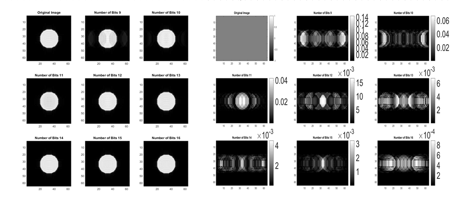
Results:
In Figure 2 the images and the error in the image are shown. For 16 bit PWM calculated error decreased below 0.1%. In Figure 3 gradient error vs bit resolution is shown. For 15 bits resolution error decreased to 3.6%. In Figure 4 simulation results from model sim is shown. It is shown that using IODELAY elements PWM signals can be generated with resolution lower than 80ps.Discussion and conclusion:
With the advancements in the transistor field higher switching frequencies are possible for full bridge amplifiers. High frequency switching requires precise timing adjustment for control signals. In this abstract it is shown that PWM signals can be generated with temporal resolution less than 80ps, which corresponds to 15 bits for a 500kHz carrier frequency of a PWM signal. It is also shown that 15 bits resolution is sufficient enough to generate desired pulses with less than 3.6% error in area, which can be reduced by adjusting timings of the gradients.Acknowledgements
No acknowledgement found.References
[1] Ertan, Koray, et al. "A z‐gradient array for simultaneous multi‐slice excitation with a single‐band RF pulse." Magnetic resonance in medicine 80.1 (2018): 400-412.
[2] Ertan, Koray, and Ergin Atalar. "Simultaneous use of linear and nonlinear gradients for B1+ inhomogeneity correction." NMR in Biomedicine 30.9 (2017): e3742.
Figures