1574
Digitally Controlled High-Power Phase Shifter for B1 Shimming at 7TChenhao Sun1, Neal Hollingsworth1, Kevin Patel1, Kasra Ghadiri1, Chung-Huan Huang1, and Steven M. Wright1
1Electrical & Computer Engineering, Texas A&M University, College Station, TX, United States
Synopsis
To mitigate electromagnetic wave interference in high field MRI, RF shimming relies on the ability to manipulate the phase and amplitude of the Tx signal on each channel. The simplest approach is to change phase shifts by switching transmission lines. We propose an electronically controlled phase shifter providing eight different states of phase shifting (0°, 22.5°…...135°, 157.5°), designed to handle 1kW Tx power and is non-magnetic so that it can be used in the magnet room. Measurement demonstrate an average insertion loss of -0.94dB and an average phase error -1.35° compared with design values.
Introduction
In high field MRI, multi-channel B1 shimming has been shown to help mitigating standing wave interference [1,2]. Having an independent RF power amplifier for each channel [5] can be utilized elegantly to acquire an arbitrary phase, but it comes with a high cost. For a system that only has one or two RF power amplifiers and using power splitters to form many channels, mechanical adjustment phase shifters [3] and coaxial cables of different lengths [4] can be used to achieve required phase shifting on each path. However, the inconvenience of frequently setting these devices limits the practice of RF shimming. In this work, a digitally controlled high-power phase shifter was built to achieve rapid and remote phase shifting. The phase shifters follow a 4-way Wilkinson Power Dividers which divide power from 4 kW PAs, thus they are designed to handle approximately 1kW Tx power per channel. The phase shifter was designed to be controlled by TTL signals from a separate control system. The phase shifters, power dividers and control system are non-magnetic to work near the magnet.Method
The phase shifter consists of 3 modules in series, providing 22.5, 45 and 90° phase shifts. A transmission line module provides a 22.5° phase shift, 2 high-pass tee modules providing the 45° and 90° at 50Ω impedance. All operate at 298 MHz. Each module can be enabled or bypassed by using PIN Diodes, manipulating phase shifting allows a total of 8 different states with steps of 22.5, (0°, 22.5°, 45°, 67.5°, 90°, 112.5°, 135°, 157.5°). The diagram of the high-pass tee module and transmission line module are shown in Fig. 1 (a) (b). For the high-pass tee module, capacitors C1, C2 and inductor L together form a phase shifting module. A transmission line (TL) was used for the 22.5° phase shift because small phase shifts were inaccurate in the lumped element designs due to the parasitic capacitance of the PIN diodes becoming to the values of C1 and C2. Forward bias on PIN diode D1 with reverse bias on D2 and D3 will bypass the module, while forward bias on D2 & D3 and reverse bias on D1 will enable the module. The DC control port receives +150mA (forward) or -48V (reverse) for biasing the PIN diodes from a driver board, which is controlled by TTL signals from the control system. A 470pF capacitor is used for blocking DC signals into the RF path. To ensure good isolation between DC and RF path, a λ/5 transmission line and a 480nH inductor were used rather than a λ/4 TL due to the presence of parasitic inductance of 0.022nF capacitor (KEMET, Simpsonville, USA). λ/5 TL first moves impedance point from “inductive” short-circuit to near open-circuit point, then a 480nH inductor is used to push impedance further close to open. Thus, the measured impedance looking into the DC path is a good open-circuit for an RF signal. The complete phase shifter board is shown in Fig. 2.Results
The component values were first calculated by formulas in Fig. 1(c), where φ is phase, ω is angular frequency and Z0 is 50Ω, then fine-tuned to get the desired phase shift values. All the component values are shown in Fig. 1(d). A network analyzer (HP4395A, HP, Palo Alto, USA) was used to measure the S21 of the phase shifter for different states, which are shown in Table 1. For the eight different states, the average insertion loss is -0.9435dB. The actual phase shifting has -1.35° errors in average compared with theoretical values. The measured isolation (S21) between DC and RF path is -33dB. The phase shifter is designed to handle 1KW Tx Power.Discussion
In this work, three phase shifting modules are used to get eight different states with a step size of 22.5° to enable fine control of phase for our initial investigation. It can be easily modified to get different phase values depending on the need. If relatively coarser but broader phase shimming is sufficient, the 22.5° phase shifting module can be replaced with a 180° tee module to provide 8 states of (0°, 45°……315°). Vice versa, 90° module can be replaced by 11.25° to get even finer steps with less range (8 states now as 0°, 11.25°, 22.5°……78.75°). If both fine step and broad range are required, simply adding more modules in series based on current design will do the job, total phase shifting states will go up as 2n, where n is number of modules.Acknowledgements
Support from the Cancer Prevention and Research Institute of Texas through research grant RP160847 is gratefully acknowledged.References
[1] Vaughan et.al. Proc. ISMRM 2005, 953; [2] Collins et. al. Proc. ISMRM 2005, 874. [3] Metzger, Gregory J., et al. "Local B1+ shimming for prostate imaging with transceiver arrays at 7T based on subject‐dependent transmit phase measurements." Magnetic Resonance in Medicine: An Official Journal of the International Society for Magnetic Resonance in Medicine 59.2 (2008): 396-409. [4] Yan, Xinqiang, Zhipeng Cao, and William A. Grissom. "Experimental implementation of array‐compressed parallel transmission at 7 tesla." Magnetic resonance in medicine 75.6 (2016): 2545-2552. [5] Bitz, Andreas K., et al. Proc. ISMRM 2009, 4767;Figures
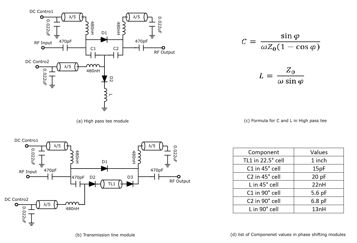
Figure 1
(a) C1, C2 and L together form a high-pass tee phase shifting module. PIN diode
D1 and D2 select enabling or bypassing of the module. 0.022uF capacitor, λ/5
transmission line and 480nH chock provide isolation between RF path and DC
path. (b) Transmission line TL1 provide the phase shifting. D1, D2 and D3
select enabling or bypassing of the module. (c) Formulas for calculating C and
L’s theoretical values for high pass tee, where ω is angular frequency, φ is desired phase shifting and Z0
is 50Ω. (d) List of components
with practical values for desired phases.
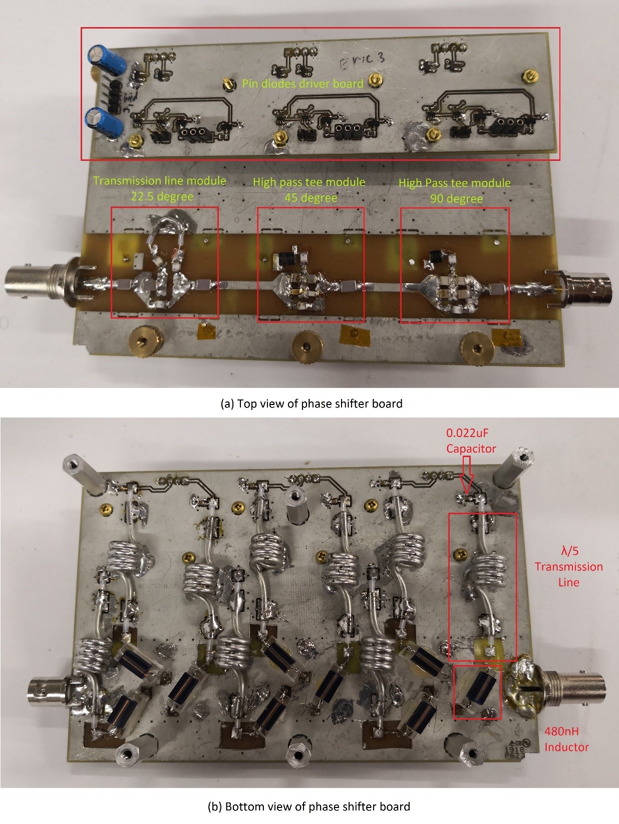
Figure 2
(a) three phase shifting module in series on top layer, from left to right 22.5°,
45°
and 90°.
A PIN diodes driver board on top provide DC control for biasing pin diodes. (b)
DC control signals from driver board go through 0.022uF capacitor, λ/5
transmission line and 480nH chock (for isolation RF signals), and go back to
top layer for biasing pin diodes.
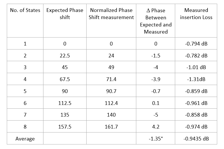
Table 1 Measurement results of different states