1559
A PIN-diode-driver for fast coil tuning using low detune currents1Experimental Cardiovascular Imaging Group, University Hospital of Ulm, Ulm, Germany, 2Research, Development and Technology (GBE), Sirona Dental Systems GmbH, Bensheim, Germany
Synopsis
To operate ultra short echo time (UTE) or zero echo time (ZTE) imaging, the ability to switch rapidly from detuned to tuned state is mandatory, as any delay causes signal loss for UTE or missing data points in the k-space center for ZTE. While propagation delays arising during radio frequency (RF) front end control can be measured and compensated, the dead time of the receive coil remains a limiting factor. In this contribution we investigated an approach to speed up PIN-diode based coil-tuning, using a dedicated driver providing a low detune current. Tuning times below $$$1000\,\mathrm{ns}$$$ could be realized.
Purpose
To operate ultra short echo time (UTE) or zero echo time (ZTE) imaging, the ability to switch rapidly from detuned to tuned state is mandatory, as any delay causes signal loss for UTE or missing data points in the k-space center for ZTE. For PIN-diode based transmit and receive (T/R) coil setups a high detune current is required to switch the transmit RF power path without distortion and minimal thermal loss. The requirement of a high detune current however is not necessarily given for receive-only coils. A standard detune circuit needs to be able to handle a certain amount of RF power, but much less then required for transmit mode. The time required for the transient state of PIN-diodes from conducting (detuned) to blocking (tuned) is given by the following equation.
$$T_\mathrm{FR} = \mathrm{ln} \left( 1 + \frac{I_\mathrm{F}}{I_\mathrm{R}} \right) \cdot \tau = \mathrm{ln} \left( 1 + \frac{I_\mathrm{detune}}{I_\mathrm{tune}} \right) \cdot \tau$$
Where $$$T_\mathrm{FR}$$$ is the transient switching time, $$$I_\mathrm{F}$$$ ($$$I_\mathrm{detune}$$$) the forward current through the diode, $$$I_\mathrm{R}$$$ ($$$I_\mathrm{tune}$$$) the reverse current and $$$\tau$$$ the minority carrier lifetime given by the PIN-diode as intrinsic property. Reducing $$$T_\mathrm{FR}$$$ can therefore be achieved by increasing $$$I_\mathrm{R}$$$ and decreasing $$$I_\mathrm{F}$$$. [1,2]
Method
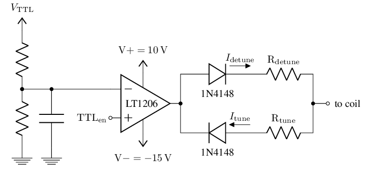
For the proof of concept a straightforwardly built PIN-diode-driver using an operational amplifier as current source/sink (Fig. 1) was used. The forward detune current was altered using a resistor matrix for $$$R_{\mathrm{detune}}$$$. The reverse tune current was set to a fixed value of $$$R_{\mathrm{tune}} = 47\,\mathrm{\Omega}$$$ limiting the maximum inrush current to $$$\approx 300\,\mathrm{mA}$$$. As only dedicated filtering element a choke coil with $$$10\,\mathrm{\text{µ}H}$$$ is included in the current path as RF block, close to the detune circuit.
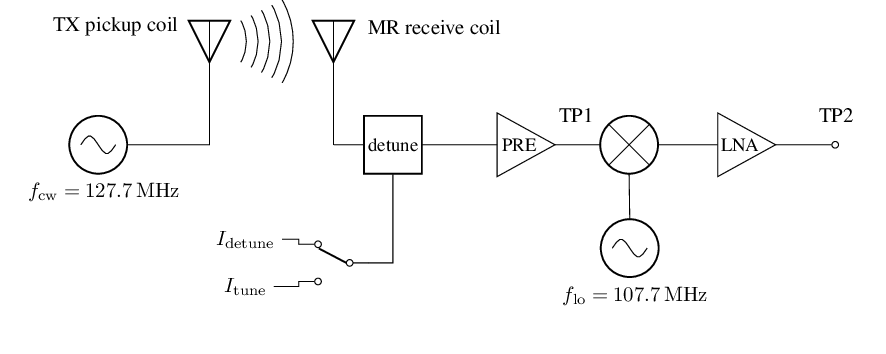
The timing behavior was measured by coupling a continuous wave into the receive coil [3], propagated over a full receive path (Fig. 2). The reduction of the transient switching time of the PIN-diode $$$T_\mathrm{FR}$$$ and the onset of the pre-amplifier (PRE) can be appreciated at the mixer input (TP1). The reduction of the total system transient time $$$t_\mathrm{tune}$$$ was measured at the output of the low noise amplifier (LNA), where the signal would be digitized (TP2).
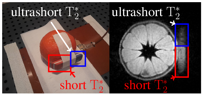
As tuned coils in the vicinity of any object would cause $$$B_1$$$ field distortion during pulse excitation, the absence of imaging artifacts can be used as an indicator for sufficient detune. The receive coil was placed underneath a phantom and detuned using different static current values, while imaging was performed using a standard Cartesian gradient echo sequence. Two regions of interest were addressed in the images, one in the direct vicinity of the receive coil (test) and one in safe distance (ref) (Fig. 4b). The image intensity of each ROI was calculated and normalized to a reference image acquired without the receive coil in its vicinity (Fig. 4a). The ratio of both, the normalized intensity $$$\left\lVert S \right\rVert$$$ was calculated, expecting a value close to 1, indicating sufficient detune.
To generally proof the feasibility of this approach 3D-UTE imaging was performed using the proposed setup for signal processing and receive.
Results
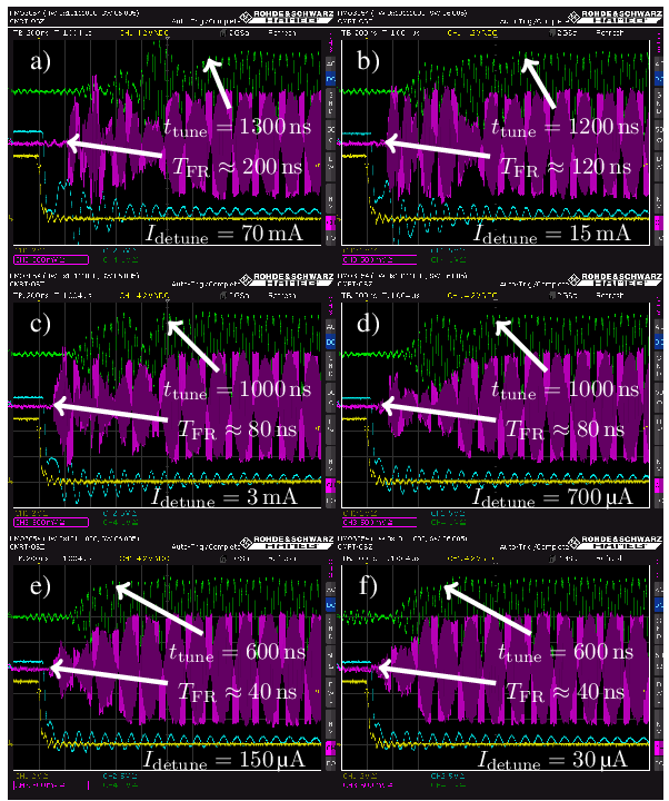
In Fig. 3 the results of the tuning measurement are plotted as follows: switching time reference (yellow), voltage over current driver output (blue), received $$$127.7\,\mathrm{MHz}$$$ carrier (red, TP1) and the down converted signal at $$$20\,\mathrm{MHz}$$$ (green, TP2). The detune current $$$I_\mathrm{detune}$$$ was reduced along the measurements from Fig. 3a - 3f. A reduced switching time $$$T_\mathrm{FR}$$$ of the diode and a reduced transient oscillation for tuning $$$t_\mathrm{tune}$$$ can be appreciated. Worst case snapshots have been selected for this plot.
For the detune test no interference can be observed for currents in the range of $$$I_\mathrm{detune} = 200\,\mathrm{mA} - 250\,\mathrm{\text{µ}A}$$$, where for each current value the normalized signal intensity ratio was $$$\left\lVert S \right\rVert = 1.02 \pm 0.01$$$. No images below $$$I_\mathrm{detune} = 250\,\mathrm{\text{µ}A}$$$ were acquired. In Fig. 4c the tuned receive coil causes heavy imaging artifacts and a normalized intensity ratio of $$$\left\lVert S \right\rVert = 0.17$$$.
The feasibility of this approach is shown by successfully performing 3D-UTE imaging shown in Fig. 5, realizing an acquisition delay, the time from the end of the excitation pulse to the beginning of signal acquisition, of $$$1\,\mathrm{\text{µ}s}$$$.
Conclusion
Based on this approach using a low detune current $$$I_\mathrm{detune}$$$, the tune delay $$$t_\mathrm{tune}$$$ could be reduced, while maintaining sufficient detune capability. In addition this setup reduces the complexity of PIN-diode-driver designs compared to other approaches. [4,5] The distinct modulation of the RF signal could be further improved by coil optimized matching of the detune current supply path, anticipating further shortening the tune delay. The feasibility of this method could also be demonstrated by performing ultra short echo time imaging with an acquisition delay of $$$1\,\mathrm{\text{µ}s}$$$.Acknowledgements
This project has received funding from the German research foundation under grant agreement RA 1960/9-1. The authors thank the Ulm University Center for Translational Imaging MoMAN for its support.References
[1] Doherty Jr., W., et al. The PIN diode circuit designers handbook, Microsemi Corporation 98=WPD-RDJ007, (1998)
[2] \Skyworks Inc. Design With PIN Diodes, Skyworks Inc. 200312D, (2010)
[3] Horneff, A., et al. An EM simulation based design flow for custom-built MR coils incorporating signal and noise, IEEE TMI 37, (2017) 527-535.
[4] Twieg M., et al. Active Detuning of MRI Receive Coils with GaN FETs, IEEE Transactions on Microwave Theory and Techniques 63 (2015) 4169-4177.
[5 Brunner D., et al. Symmetrically biased T/R switches for NMR and MRI with microsecond dead time, JMR 263 (2016)147-155.
Figures
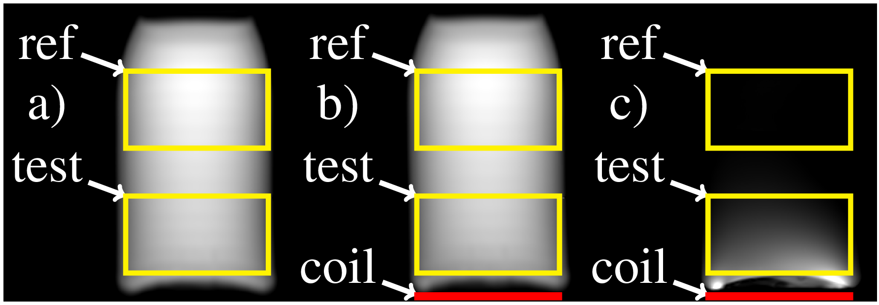
As tuned coils in the vicinity of any object would cause $$$B_1$$$ field distortion during pulse excitation, the absence of imaging artifacts can be used as an indicator for sufficient detune. The receive-only coil was detuned using different static current values. Imaging was performed using a Cartesian gradient echo sequence. Two regions of interest where investigated, one close to the receive coil and the other in safe distance. In a) the phantom without the receive coil is shown. In b) the detuned coil is underneath the phantom, no image distortion can be appreciated. In c) the tuned receive coil causes heavy imaging artifacts.