1542
Clock Transmission Methods for Wireless MRI: A Study on Clock Jitter & Impact on Data Sampling1Electrical Engineering, Stanford University, Stanford, CA, United States, 2GE Healthcare Inc, Stanford, CA, United States, 3GE Healthcare Inc, Aurora, OH, United States, 4Radiology, Stanford University, Stanford, CA, United States
Synopsis
Creating wireless MRI receive coils requires the clock for the on-coil electronics to be in phase with the clock of the MRI transmit system. Sending a wireless clock using a phase locked loop (PLL) single tone that is divided down versus a dual tone AM double side band suppressed carrier (AM DSB-SC) system can have different results in jitter of the clock. We experiment with these architectures,. The wireless clock transfer methods will ultimately impact SNR of the ADC system and its robustness to phase changes from environmental scenarios such as patient motion or multipath effects.
Introduction
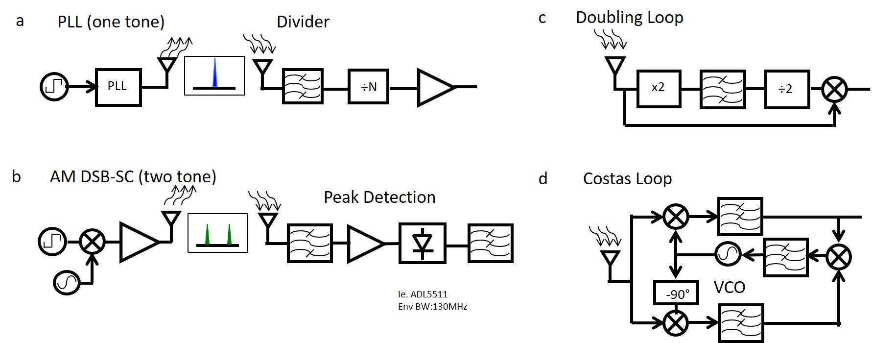
One challenge in developing wireless MRI receive coils is wireless clock transmission to on-coil electronics (ie ADC). Clock drift between transmit and receiver electronics will create image artifacts1-2. The system must maintain clock accuracy despite path loss, antenna impedance changes, multipath interference from patient/bore reflections, and breathing motion. This work experiments with two wireless clock transfer and recovery methods: a PLL generating single tone with frequency division at receive (Fig 1a) and dual tone AM DSB-SC (double sideband suppressed carrier) with peak detection at receive (Fig 1b). The recovered clocks provided the sampling clock to an ADC and the resulting SNR values were compared. Additionally, we address subtleties in function, and performance.Theory and Considerations
The PLL/divider method is effective in dividing down clock phase changes due to coil motion (ie patient breathing). Although a digital N divider reduces phase noise by 20log10(N)dB, input broadband noise and spurs may alias onto the output frequency fout, adding additional 10log10(BW/(2fout)+1)dB noise3, where BW is the input noise bandwidth. Filtering before the divider mitigates this.
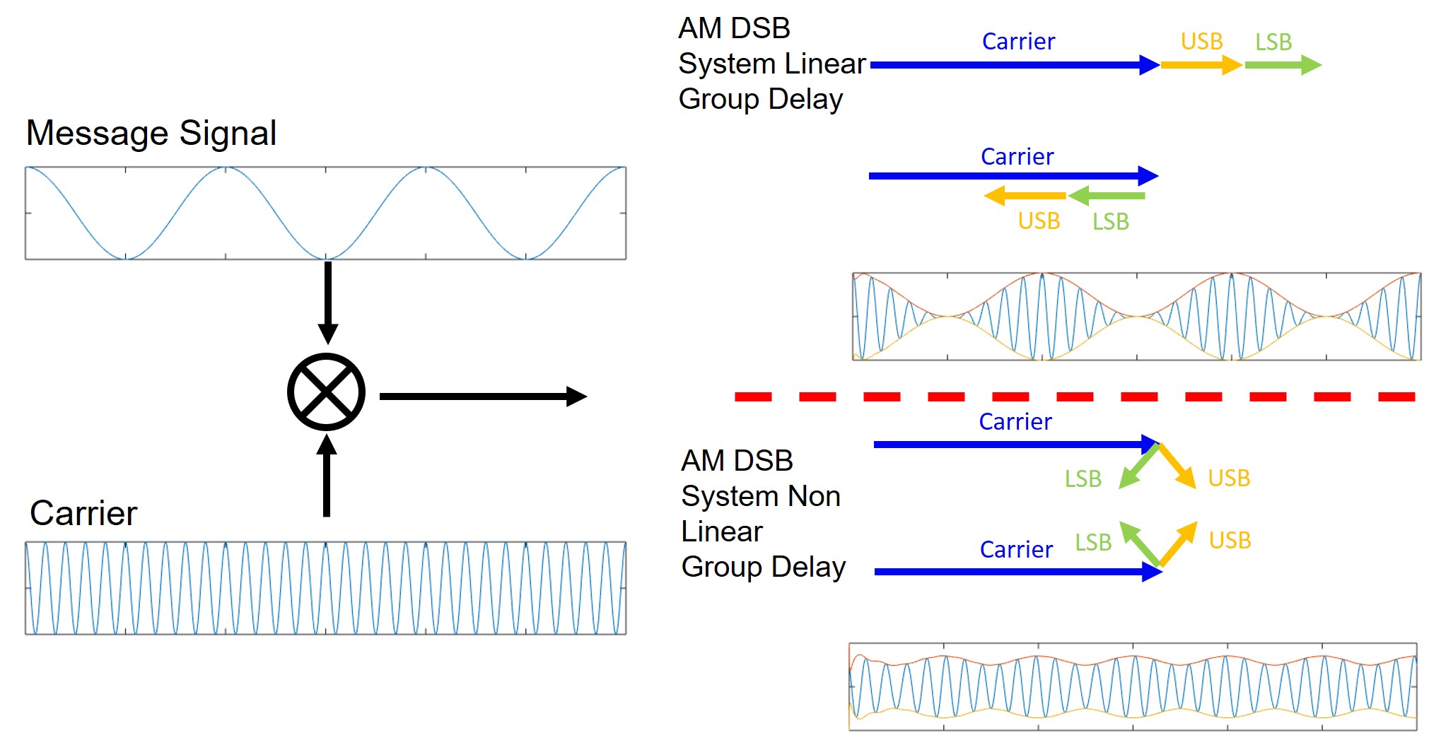
A suppressed carrier AM signal (equivalently, binary phase shift keying BPSK) is more robust than AM with carrier in systems having nonlinear group delay. In full AM, if the sidebands become orthogonal to the carrier, peak detection fails (Fig 2). With clock frequencies of 10MHz or higher, group delay is unlikely to be linear. AM DSB-SC avoids this, and peak detection output yields double the input frequency. Additional receivers including squaring loop (Fig 1c) and Costas loop (Fig 1d) architectures are feasible but unnecessary due to simplicity of the binary phase shift keying (BPSK) clock signal.
Materials and Methods
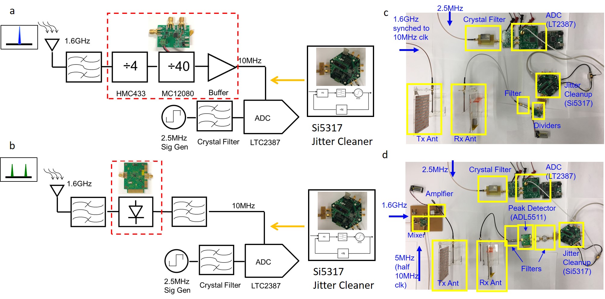
We used an 18-bit LTC2387 SAR ADC that samples up to 15Msps to mimic on-coil clock jitter tests. Our experiments sample at 10Msps. A signal generator (Keysight 33600A Series) generates a 2.5MHz waveform that is crystal filtered and fed into the ADC input. A clean, higher frequency input allows more observable jitter effects of wireless clock transmission that limit k-space peak SNR.
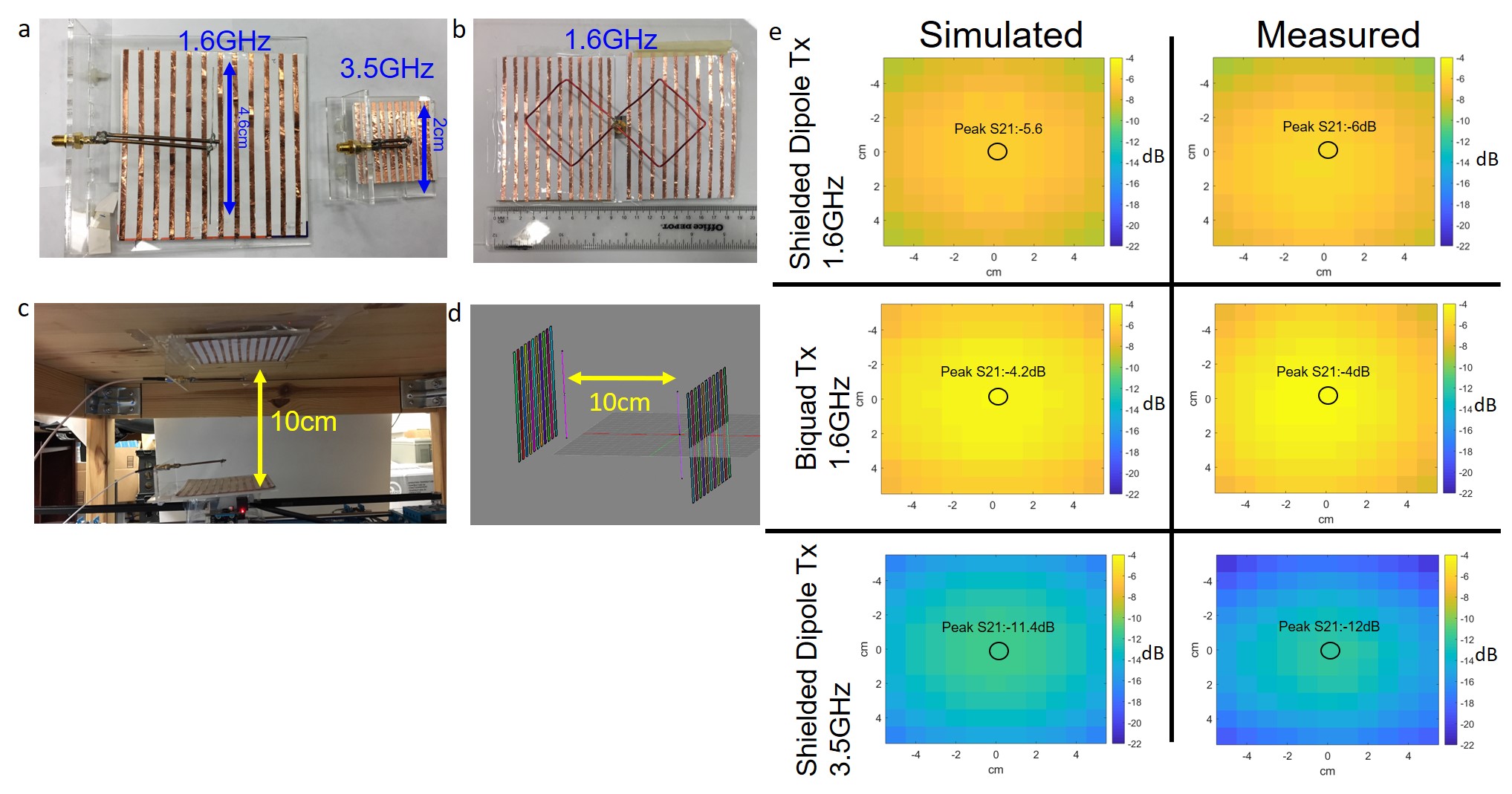
We constructed a set of 1.6GHz and 3.5GHz strip shielded dipole antennas, and a 1.6GHz biquad antenna (Fig 3). Path loss across a parallel plane 10cm away was simulated and measured by robotic XY plotter. Two strip-shielded 1.6GHz dipoles were ultimately used for wireless clock transfer (Fig 4c,d).
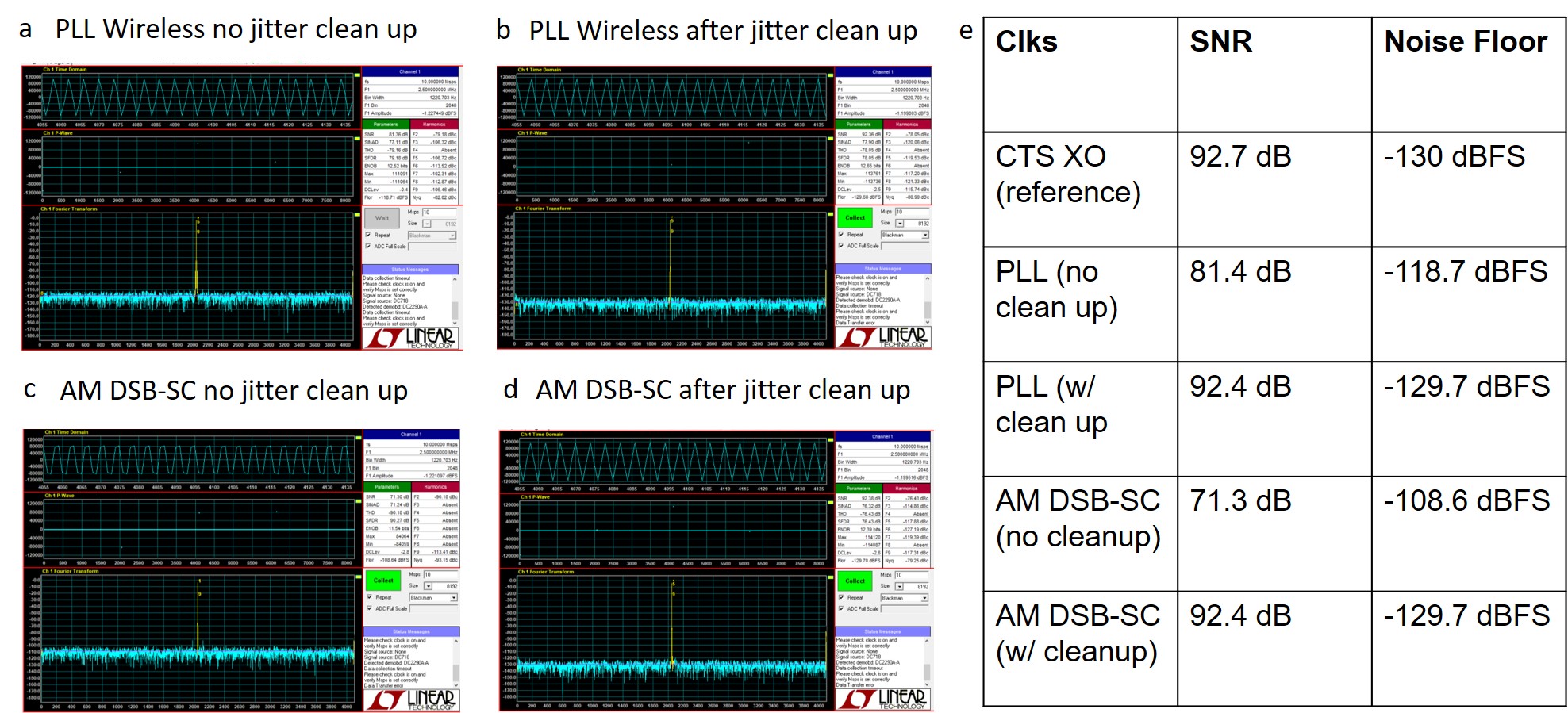
In the first setup, a signal generator (E4420B) wirelessly sends a 1.6GHz tone across 10cm where it is divided down to a 10MHz clock for the LTC2387 ADC (Fig 4a, 4c). The second test mixes (LTC5560) a 5MHz signal with 1.6GHz before transmission, after which peak detection retrieves the clock at original 10MHz (Fig 4b,4d). Pscope data collection software (Linear Technologies) records the ADC SNR values and noise floor. Additionally, a jitter cleanup circuit (Si5317) (center freq=10MHz, BW=88Hz) was inserted after each receiver and SNR improvement recorded for comparison. The ADC SNR using a 10MHz crystal oscillator (Crystek Corporation) was recorded as a gold standard measurement.
Results and Discussion
The path loss varies between -5 to -10dB between two 1.6GHz shielded dipole antennas when displacing Rx antenna across a 10cmx10cm plane 10cm away. Simulation values agrees within 1dB. A higher frequency transmission between the 3.5GHz shielded dipole antennas result in greater path loss: -11dB to -20dB. At 10cm distance, the 3.5GHz antennas operate in the far field, while the 1.6GHz antennas are in the near/mid field region. The 1.6GHz antenna impedance thus may modulate more from patient motion, but with reduced path loss.
The PLL/divider approach results in 81.4dB SNR, an 11dB reduction relative to the crystal clock standard. The divider recovery phase will be sensitive to both antenna impedance and path length changes. The AM DSB-SC/peak detection achieves 71.3dB, a 21.4dB reduction from the crystal standard. Future low noise peak detection circuitry may improve this outcome. The AM recovered clock phase is influenced by envelope group delay and should mitigate antenna impedance modulation. For either clock recovery scheme, the Si5317 brought the ADC SNR back to ~92dB. Importantly, this jitter attenuator does not employ an external VCO (only fixed clock) so that voltage sensitive clock modulation from pulsed gradients could be limited.
Conclusion
Wireless clock transmission at 1.6GHz resulted in reasonable path loss across a perpendicular plane 10cm from the clock receiver. Wireless clock transmission using PLL/dividers and AM DSB-SC degraded the SNR relative to direct crystal ADC clocks, but SNR can be remedied with jitter cleanup. Further studies are needed to determine phase stability of these wireless clock transmission methods with patient motion and vibration effects.Acknowledgements
The authors thank GE Healthcare Research Support, NIH Grant R01EB019241, the Stanford Graduate Fellowship and National Science Foundation for funding sources.References
[1] Lu J, et al Wireless Clock Transfer for MRI Phase Correction, 25th ISMRM, 2017
[2] Bosshard J, et al Phase Correction with Asynchrnous Digitizers, 23rd ISMRM, 2015
[3] SenGupta, A Effect of Aliasing on Spurs and PM Noise in Frequency Dividers, IEEE International Frequency Control Symposium and Exhibition, 2000
Figures