1536
Universal WiGig MRI receiver platform with auto-synchronised clock module and ZYNQ-based high-speed digitizer1Institute of Neuroscience and Medicine - 4, Forschungszentrum Juelich, Juelich, Germany, 2Institute of Neuroscience and Medicine 11, INM-11, JARA, Forschungszentrum Jülich, Juelich, Germany, 3JARA - BRAIN - Translational Medicine, Aachen, Germany, 4Department of Neurology, RWTH Aachen University, Aachen, Germany
Synopsis
The operation of 60GHz data
transmission inside the MR room using the WiGig standard has been demonstrated
in a previous study. It offers an off-the-shelf solution for reliable,
high-speed data transmission as required by modern high-channel-count array
coils. However, wireless data transmission is only one component of a complete
receiver chain in MRI. Since the ARM-based platform employed in our previous
study is not powerful enough to implement full high-speed high-fidelity
acquisitions, we propose to connect the WiGig data link with a FPGA board,
clock generator board and a high-precision ADC board to increase the speed and the
fidelity.
Purpose
The operation of 60GHz data transmission inside the MR room using the WiGig standard has been successfully demonstrated in a previous study1. It offers an off-the-shelf solution for reliable, high-speed data transmission as required by modern high-channel-count array coils. However, wireless data transmission is only one component of a complete receiver chain in MRI. Since the ARM-based platform employed in our previous study1 is not powerful enough to implement full high-speed high-fidelity acquisitions, we propose to connect the WiGig data link with a field programmable gate array (FPGA) board, clock generator board and a high-precision ADC board to increase the speed and the fidelity.Methods
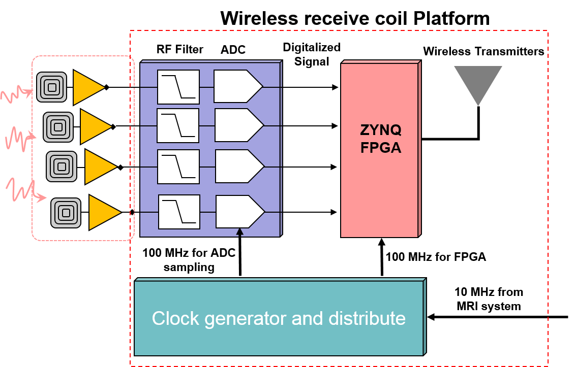
Fig 1. shows the arrangement of the proposed wireless MRI receiver platform arranged around a ZYNQ FPGA (ZCU104, Xilinx, USA) board. A high clock rate, high-resolution ADC (LTC2195, Analog devices, Norwood, USA) was used for digitizing the signal received from the coils. The FPGA currently supports basic ADC control and data-buffering. In the future, high-speed signal processing modules, such as digital down-conversion (DDC) and digital filtering, will be added. In addition, an ARM core was implemented inside the FPGA, which is used for data packing and universal interfacing (USB) to the wireless module. The in-house built clock module is driven by a reference clock from the MR system and generates the sampling clock for the ADCs. This architecture has been chosen to maintain phase coherence with receive signal processing in the MR system itself. The WiGig dongle has already been verified in a previous study1.
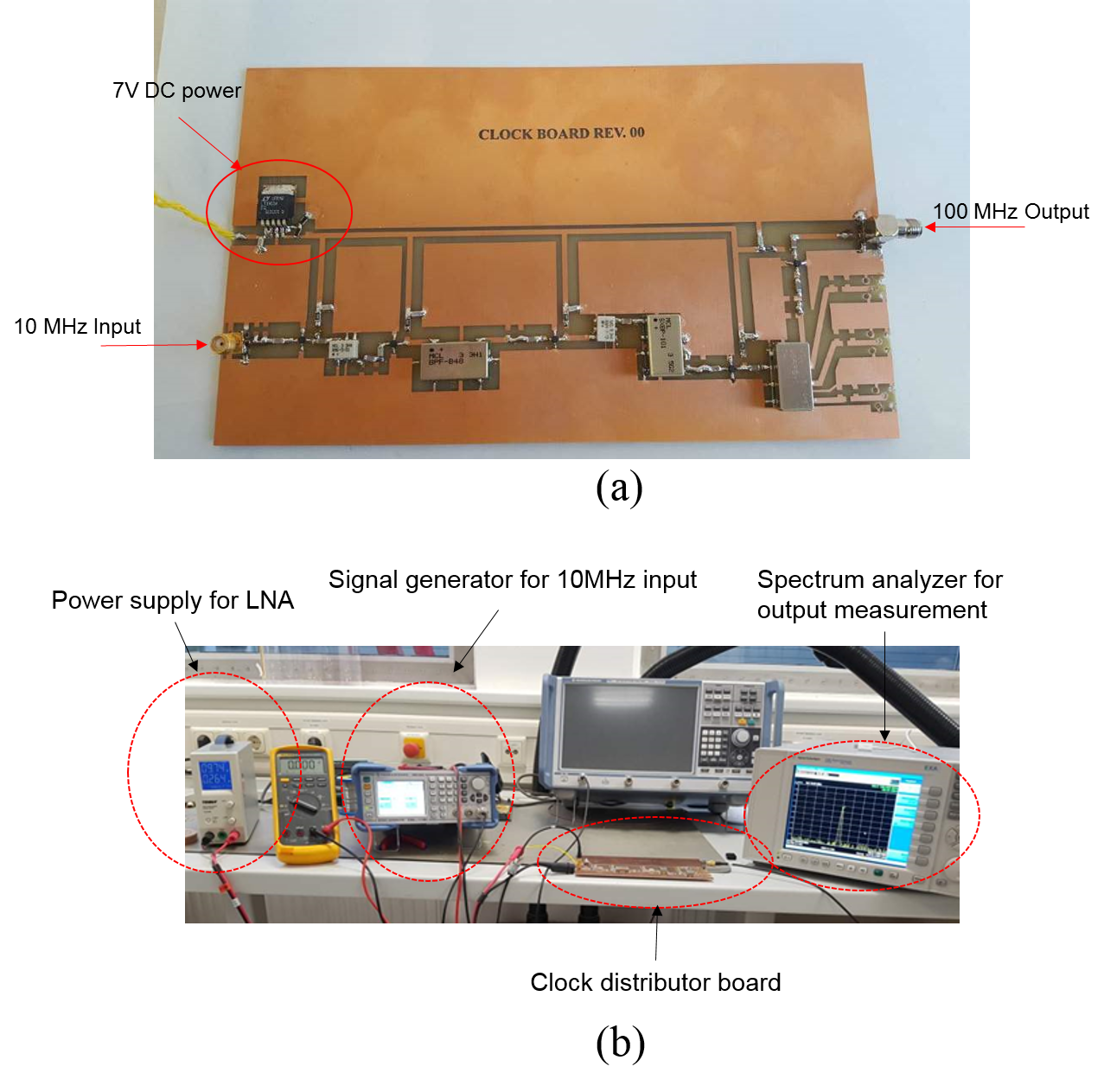
The SNR of ADC is related to the sampling clock jitter2. It means that the clock generator module should be optimized for low jitter performance. In this work, we implemented a clock generator and distribution system on a double-layer FR4 PCB, as shown in Fig. 2(a). The clock module up-converts the MR system’s 10 MHz clock to a 100 MHz clock signal, which drives the ADCs. The clock generator board was tested on the bench, as shown in Fig 2. (b). In the lab setup, the linear regulator (LT1963, Analog devices, Norwood, USA) was driven from a lab DC power supply 72-834 (TENMA, Aschheim, Germany). The reference signal was generated by a SMC100A (Rohde & Schwarz) signal generator. The jitter performance of the clock module was evaluated with a spectrum analyser N9010A (Keysight Technologies, Santa Rosa, USA).
Results
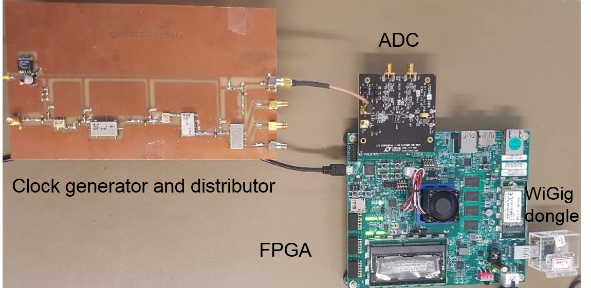
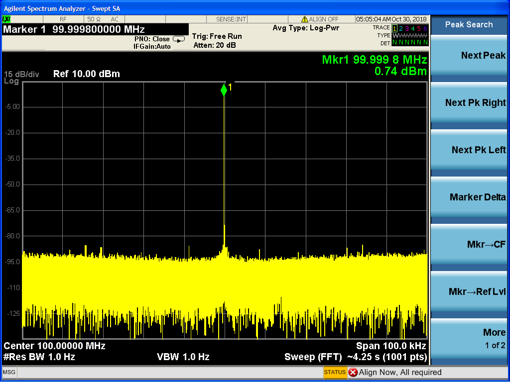
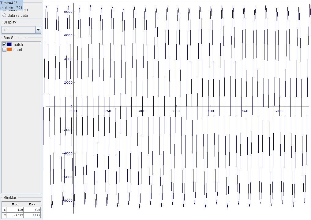
Fig. 3 shows the implemented wireless receiver platform. It contains the ZYNQ FPGA, the 16-bit 125Msps ADC board, the home-built clock generation and distribution board, and the WiGig dongle (MR.loop, Taiwan) used for wireless data transmission. The measured output clock of the clock generator board is shown in Fig. 4. The clean 100 MHz clock for the ADC sampling was generated from the 10 MHz input clock. The setup was used to acquire and digitize a 125MHz sine signal. 125MHz data can be digitalized by the 100 MHz sampling clock using an under-sampling method3. The measured phase noise was 86 dBc (1kHz offset), 88 dBc (100kHz offset), and 118 dBc (1MHz offset), respectively, which was similar to that of the source frequency (10MHz). Fig. 5 shows the captured digitalized signal into FPGA of the proposed platform. The acquired signal is captured by the Chipscope™ Integrated Logic Analyser (ILA) core in Vivado software provided by Xilinx Inc. (San Jose, USA).Discussions
We have proposed a WiGig based MRI receiver platform using a commercial ADC, FPGA board, and a WiGig dongle, as well as a customized clock generator board. Digital wireless transmission of the MRI receive signal is feasible based on the preliminary evaluation of the platform. The direct digitalized ADC has the advantage of having a simple receive structure because it does not require an analogue down converter mixer and IF bandpass filter. This would be a better solution for MRI applications such as multiband acquisition and multi-channel receiver arrays, with reduced DC and ghosting artefacts4. For future study, digital signal processing and digital data packaging will be performed on the ZYNQ FPGA, including ADC data buffering and digital processing (down-converting, filtering) in the FPGA fabrics while file formatting and USB interfacing will be accomplished with the use of an ARM core also implemented on the FPGA.Acknowledgements
We would like to thank Claire Rick for proofreading, and Annette Weber for her assistance in preparing the PCBs used in this study.References
[1] Y. Ko, W. Bi, J. Felder, N. J. Shah, "Wireless Digital Data Transfer using Millimetre-Waves in MRI system," ESMRMB; 2017.
[2] T. Neu, "Clock jitter analyzed in the time domain, Part 1," Analog Applications, 2010.
[3] P. Poshala, “Why oversample when undersampling can do the job?”, Texas Instruments application report, 2013.
[4] S.Hashimoto, "Comparison of analog and digital transceiver systems for MR imaging," Magnetic Resonance in Medical Sciences, 2014.
Figures