0574
Out-phasing Modulated Current-Mode Class D (CMCD) Amplifier with Improved Dynamic Range1Biomedical Engineering, Case Western Reserve University, Cleveland, OH, United States, 2Hyperfine Research, Guilford, CT, United States, 3Radiology, Case Western Reserve University, Cleveland, OH, United States
Synopsis
Developments in RF transmit systems have been trending towards increasing independent elements and compact designs. Previous work has shown the capability of enhancement mode Gallium Nitride (eGaN) FETs in high-efficiency switchmode RF amplifier (RFPA) based on envelope elimination and restoration (EER). Switchmode RF amplifiers, however, suffer from nonlinearity and limited dynamic range, leading to errors in excitation profiles. Here we present preliminary results on a new prototype which adds an additional modulation methods using digital controls to increase RFPA dynamic range.
Introduction
Recent developments have shown that placing transmit amplifiers on-coil and using high-efficiency amplifier topologies will allow implementation of high-density arrays with independent transmit elements1-6. Switch mode RFPAs have high in efficiency yet are inherently nonlinear; there are various methods that can increase linearity, such as drain bias modulation and gate modulation7. The previous version of the CMCD RFPA has relied on envelope elimination and restoration (EER)8 that gives the amplifier a dynamic range of 36 dB2-3,6. The limitation (see figure 1) is imposed by the minimum duty cycle of the Buck converter (Class S Amplifier) biasing the CMCD stage. This leads to a sharp cut off on the output waveforms which can affect the performance of the slice profile. We present here a system that allows out-phasing modulation in addition to drain modulation to increase the dynamic range of the CMCD RF amplifiers.Method
Board modification: The current version of eGan FET CMCD RFPA, which operates at 123.23Mhz, (Figure 2) is a more compact design based on previous iterations1-4,6 which used EER for output amplitude modulation. A digitally programmable variable delay (SY89295U) was added to one of the gate drivers which shifts the logic signal from 0 to 180 degrees out of phase from the signal going into the other gate driver. Unlike previous work, which needs pre-amplification of the gate signal, outputs of the variable delay can be directly interfaced with the gate driver in this prototype. By varying relative phase shift between the gates, the output power can be modulated9-10 in addition to EER. While this could potentially be used to modulate the waveform over the entire power range, out-phasing modulation has very poor efficiency, and thus it is only used near to modulate at low output power levels.
Out-phasing: All experiments are performed using a customized 16 channel coupled network analyzer11. For out-phasing, one PXI-6355 module is used to output 5 lines of digital waveforms for controlling the out-phasing circuit. A MATLAB script generates digital output waveforms for each line along with the RF pulse waveforms which LABVIEW plays out simultaneously. This set up allows us to change the envelope dynamically to modulate the RF pulse.
EER has limited minimum output based on the minimum on time of the PWM at the buck converter. Below this threshold, control must be switched to out-phasing modulation (Figure 4a). Therefore, steady-state output power is calculated in this fashion, allowing us to map the dynamic range of the new prototype. Here we explore dynamic modulation, using both EER and out-phasing control simultaneously. Digital waveforms are calculated to mitigate output behavior below threshold. A sync pulse with a very small peak amplitude (-5dBm) was synthesized using both out-phasing and drain modulation. This experiment shows the capability of out-phasing to create pulses that previous versions could not.
Results
Modified RFPAs have a maximum output power of 50 dBm and maximum efficiency of 79%. Out-phasing is known to reduce power efficiency more severely than drain modulation8. Therefore out-phasing is only implemented at low power levels, thus preserving high efficiency at high output power.
Figure 3. demonstrates the ability of out-phasing to modulate the RFPA response. Data is acquired for three drain bias voltages ($$$V_B$$$). Therefore, this multidimensional control needs to be mapped in order to create desired profiles. For simplicity, we’ve determined an input threshold where the main control mechanism is switched between drain bias modulation and out-phasing as described in Figure 4a. Figure 4b shows the summary of this experiment where the modulated signal is able to approach the minimum detection threshold and the dynamic range is increased by 22 dB from the previous version.
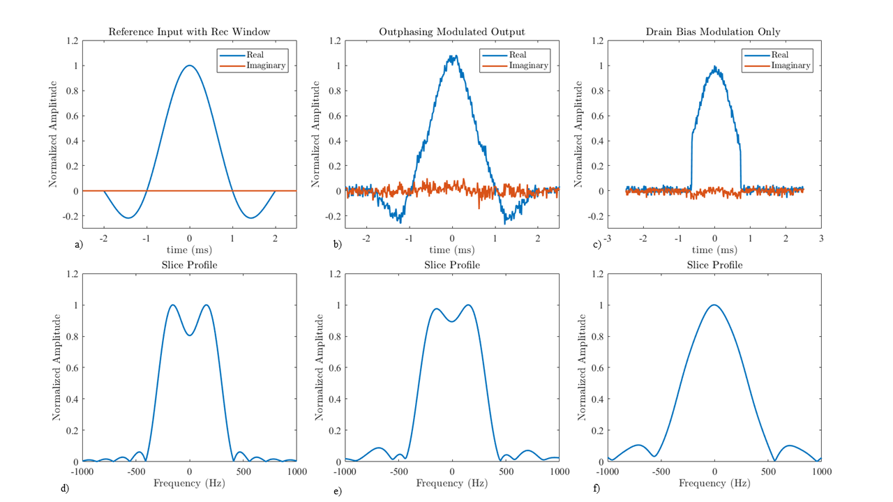
Figures 5b and e show the out-phasing modulated output in response to a reference low amplitude sinc pulse shown in figure 5a. A majority of the waveform is modulated by out-phasing since it’s below the threshold. Out-phasing is able to recreate a pulse in the time domain that follows closely with the reference. Furthermore, the slice profile has a similar performance than the reference as well, with a slightly higher side lobe. Both the time domain response and slice profile of the modulated output outperformed the not modulated output.
Discussion and Conclusion
We have implemented dynamic digital control of the gate waveforms. This adds another degree of control for controlling the output power, increasing the total dynamic range of our CMCD RFPA to 59 dB. In the future, we aim to map the phase to output response in higher resolution as well as add more bias points to create a dictionary of the output response with respect to both modes of control. This would allow automated digital waveform calculation for envelope modulation.Acknowledgements
This material is supported by Siemens Healthineers and the National Science Foundation Graduate Research Fellowship Grant No. CON501692.References
- Twieg, M. et al. Enhancement Mode GaN (eGaN) FETs for On-Coil MRI Transmit Amplifiers. 21st ISMRM (2012)
- Twieg, M. & Griswold, M. A. High efficiency radiofrequency power amplifier module for parallel transmit arrays at 3 Tesla, Magnetic Resonance in Medicine, Oct. 2016.
- Twieg, M. & Griswold, M.A.Optimizing the Current-Mode Class D (CMCD) Amplifier for Decoupling in pTX Arrays. 23rd ISMRM (2015).
- Gudino, N. et al. On-coil multiple channel transmit system based on class-D amplification and pre-amplification with current amplitude feedback. Magn Reson Med 70, 276–289 (2013).
- Gudino, N. et al. Optically controlled switch-mode current-source amplifiers for on-coil implementation in high-field parallel transmission. Magnetic Resonance in Medicine 76, 340–349 (2016).
- Twieg, M. D. Applications of Gallium Nitride FETS to RF Arrays for Magnetic Resonance Imaging. (Case Western Reserve University, 2016).
- Ashfaq, B. et al, A Gate Modulated Digitally Controlled Modified Class- E Amplifier for On- Coil Applications in 1.5 T MRI. 26th ISMRM (2018)
- Kahn, L. R. Single-Sideband Transmission by Envelope Elimination and Restoration. Proceedings of the IRE 40, 803–806 (1952)
- Chireix, H. High Power Outphasing Modulation. Proceedings of the Institute of Radio Engineers 23, 1370–1392 (1935).
- Cox, D. Linear Amplification with Nonlinear Components. IEEE Transactions on Communications 22, 1942–1945 (1974).
- Twieg, M. & Griswold, M. A. 16 Channel Coupled Network Analyzer for Characterizing pTX Systems at 3T. 26th ISMRM (2018).
Figures